New imaging method to assess quality of 3D-printed metal parts
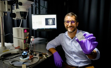
Scientists from NTU Singapore have developed a fast imaging system to analyze the inner structure of 3D-printed metal parts.
Scientists from NTU Singapore have developed a fast imaging system to analyze the inner structure of 3D-printed metal parts.
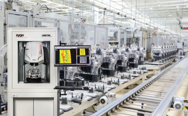
Zygo is constantly researching and refining interferometry-driven optical metrology tools and recognizes that digital holography is gaining significant momentum in the measurement of surface topography due to increases in the speed and data capacity of today’s computers.

Corning has launched a dicing technology that will allow the company’s laser technologies business to enter the semiconductor application space to further focus on microfabrication processes.
As a leading component manufacturer, Hamamatsu is well aware of the advantages and disadvantages offered by various systems, and the main differences will be explained in the new issue of PhotonicsViews, 1/2022.
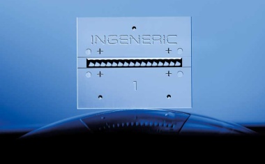
In order to give developers of microlens arrays (MLAs) the opportunity to sound-out the potential of this technology, Ingeneric presents an MLA demonstrator in a new technical article in PhotonicsViews issue 1/2022.
Issue 1/2022 – February / March – is online and has been mailed. It includes feature articles from Cailabs, Coherent, Hamamatsu Photonics, Ingeneric, iPronics, Joya Team, Solmates, and more companies and institutions. On the cover: Shenzhen JPT Opto-Electronics.
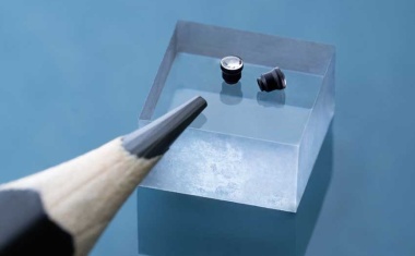
Highly precise 3D structures in black can now be printed using a 2-photon polymerization (2PP) 3D printing process. This seemed for a long time impossible as non-transmissive (black) materials greatly reduce the polymerization efficiency of the printing process.
Technical article by Lea Sauerwein, Christian Ebenhöh, and René Geiger in the current issue 5/2021 of PhotonicsViews: a new approach to the joining of polymers combines two different processing wavelengths with the method of quasi-simultaneous welding in order to achieve a significant reduction of welding time and enhanced weld seam quality.
Technical article by Patrick Kim in the new issue 5/2021 of PhotonicsViews: new laser system component minimizes unwanted heat accumulation in the material being processed compared with traditional CO2 laser sources, which typically produce longer pulse rise/fall times of approximately 60 μs.
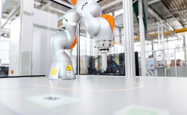
The safety of people interacting with robots has top priority, especially when humans and robots are working side by side instead of being separated from each other by safety fencing. The Fraunhofer Institute for Factory Operation and Automation IFF’s web-based design tool helps companies design their cobots. The Cobot Designer helps minimize the risk of accidents and increases employee safety. The tool is available as a free web application.
Peter J. de Groot and Michael Schmidt have provided a pivotal article, looking at the extremely important subject of the role of metrology in Industry 4.0.

By analyzing lens data during optics design, the optimal optical fabrication chain can be determined.
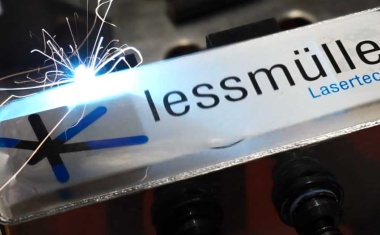
One of the key laser application areas in the e-automotive industry is the welding of the battery. Sensor systems from Lessmüller Lasertechnik ensure reliable high-precision joining, which is vital in the assembly of any battery. Installed to various remote and fixed welding optics, the OCT, WELDCHECK, and WELDEYE sensor systems demonstrate real-time monitoring capability with great accuracy and over a wide dynamic range, enabling faster, cost-effective e-automotive laser processes and streamlined production.
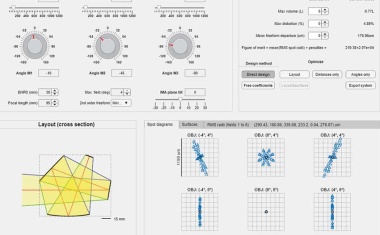
Researchers at Brussels Photonics, Vrije Universiteit Brussel, have developed a “first time right” design method that eliminates the “step-and-repeat” and “trial-and-error” approach in optical system design. They demonstrated the systematic, deterministic, scalable, and holistic character of their disruptive technique with various freeform lens- and mirror-based high-end examples and invite optical designers to experience their new method hands-on via an open-access trial web application.
The welding of glass with ultrashort-pulsed lasers (USP) is usually conducted with microscope objectives. Their short working distance limits the thickness of the work piece, the usable laser power and the feed rate of the process. To increase the possible dimensions of the welding partners and the process speed to industrial levels, a research team from Jena presents USP welding with a galvoscanner and a common F-theta lens. In a new article, they discuss differences between the well-known breakdown regime and the filamentation regime, and show tensile measurements.
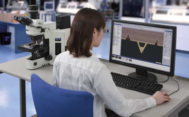
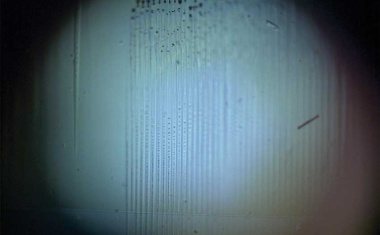
One of the factors that contributes to the recent considerable reduction in the size and high integration of electronics and other devices it is the miniaturization of the electronic components that they contain. In addition, new fine functional materials have been developed and widely used in industrial fields including the automobile, aviation, metal, and chemical industries. As a result, higher accuracy and resolving power are required for minute three-dimensional measurement of these components and materials. Although a variety of devices are available to satisfy these requirements, the confocal microscope is gathering attention as the device of choice for easy three-dimensional, non-contact surface profile measurements in air.
Disinfection processes are of particular interest due to growing concerns over illnesses caused by microorganisms and the persistent problem of healthcare acquired infections. Additionally, because of the rise of antibiotic resistant bacteria, the investigation of novel non-antibiotic approaches for the prevention of infectious diseases has become highly topical. Blue light disinfection is such an approach and light-emitting diodes (LEDs) with an emission maximum in the range of 405-nm wavelength represent an attractive light source for this.
PhotonicsViews chosen as official publishing medium for Photonics Germany – Spectaris and OptecNet Deutschland – and DGaO
Alliance for optical technologies and quantum technologies in Germany

Jürgen Popp: Light offers solutions to tackle infectious diseases