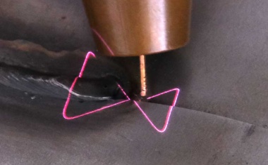
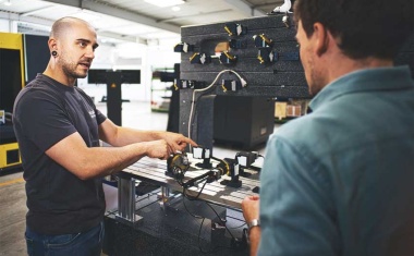
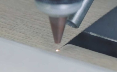
High speed laser cutting of EV electrodes
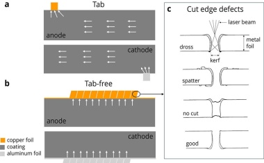
High-quality cut edges are essential to ensure reliable electric connections and prevent defects like spatter and dross, which can cause internal short circuits.
High-quality cut edges are essential to ensure reliable electric connections and prevent defects like spatter and dross, which can cause internal short circuits.
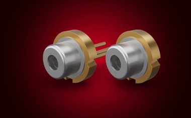
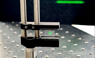
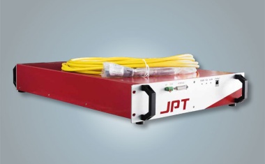
Product: High-power and high-volume Pulsed Laser Diodes (1550UA Series) at 1550 nm
A new early view article in PhotonicsViews discusses challenges for busbars in mass production, and high-speed CO₂ laser busbar de-coating methods.
A new article in PhotonicsViews discusses the production of high-quality oxides-based optical filters with low losses.
A method for improving the narrow-axis integrated intensity uniformity in laser line beam shaping for partially coherent laser sources is presented in the PhotonicsViews e-Special 1/2025.
A new early view article in PhotonicsViews presents a rigorous far-field model that allows to calculate the reflectance of the via.
A qualitative and quantitative analysis of ultrashort-pulse processing of glass in a technical article – now online and in PhotonicsViews issue 1/2025.
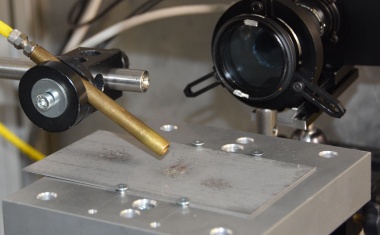
Insect residues disturb and interrupt the laminar air flow on airplane wings after a while. These residues therefore need to be repeatedly removed. Shockwave-based laser cleaning of insect residue on stainless steel (1.4544.9) is presented in an early view article in PhotonicsViews.
Faced with advancing climate change, we drastically need to monitor and understand the various sources and sinks of greenhouse gases worldwide in real time. One approach to accomplishing this is to regulate and monitor man-made methane emissions. Laser systems as developed by researchers at Fraunhofer ILT offer ways to do exactly that. At the heart of lidar instruments, they can precisely determine greenhouse gases in the atmosphere with high spatial and temporal resolution, even from great distances, and do so worldwide.
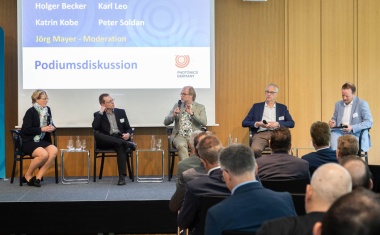
The opportunities and challenges of photonics and quantum technologies were addressed at the Photonics Germany Future Summit in Berlin.
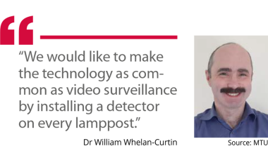
A new gas-sensing network that analyzes multiple gasses in real time in towns and cities is being developed to prevent deaths caused by ambient air pollution.
Experts from Lessmueller Lasertechnik discuss the advantages to extend the use of OCT – as known from laser welding – to classical GMAW in an early view article of PhotonicsViews.
Individualization, shorter product cycles and prototyping are leading to increased use of additive manufacturing in industry. A reliable and versatile process like laser plastic welding is needed to join parts with other additively manufactured or injection molded parts.
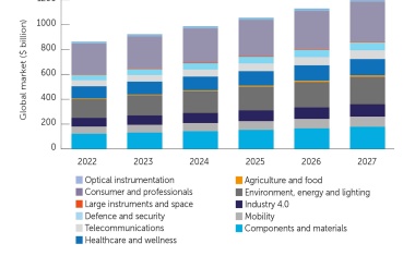
New research published today shows the photonics industries in Europe, the US, and Asia outpaced global GDP from 2019 to the post-pandemic period of 2022, growing at a CAGR of 6.8 %.
Quantum technologies: Bosch aims to use sensors to take a leading position, describes areas of application from medicine to mobility in a new PhotonicsViews article.

Nanoscale semiconductor particles are making waves in the sectors including autonomous vehicles, food inspection, medical devices, artificial intelligence, and more, as industry players increasingly seek to expand their access to infrared data.

KDPOF and Trumpf describe the implementation of optical data communication standards and solutions for the automotive industry in a new technical article.
With its immense computing power, quantum communication is set to become the backbone of the next-generation internet.
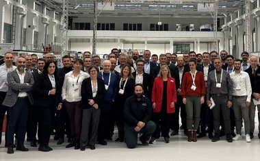
During a two-day meeting hosted by the University of Stuttgart at the cutting-edge research campus ARENA2036, a panel of experts discussed the latest developments, new applications, and market trends.
In recent years, kilowatt lasers have become standard products in the industrial laser market. The popularity of kilowatt lasers has greatly improved the efficiency and capabilities of industrial processing. Despite the performance improvements, the large size of these lasers has posed significant challenges in transportation and assembly. As a result, laser manufacturers have contemplated ways to reduce the overall size of these laser systems.
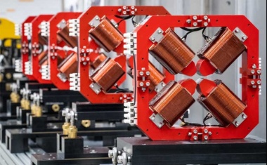
How do you measure the temperature of individual atoms at an altitude of ninety kilometers?
Laser companies present solutions to counteract the health hazards posed by particulate matter as required by the new EU vehicle emission standard, Euro 7.
National Science Foundation awards 90.8 million dollars to Arizona State University to advance x-ray science.

New project to advance perovskite-based optoelectronics, such as solar cells, photodetectors, and LEDs.
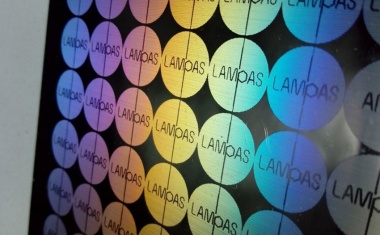
Project LAMpAS presents the first laser system that can achieve controlled topographic characteristics.
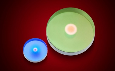
Laser Components has further optimized its processes for manufacturing and inspecting graded reflectivity mirrors (GRMs) – so-called Gaussian mirrors.

The new product line expands Coherent’s existing DOE technology consisting of industry leading volume and surface Bragg gratings with applications in communications and medicine.
A consortium led by the University of Amsterdam received a €7.5M Horizon grant to make quantum clocks more robust and compact.
The ATSM project developed an optics module and control software for laser-based production of tribological multilayer systems. PhotonicsViews has the interview with project manager David Pallasch.
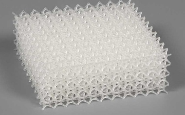
Nanoscribe’s 3D microfabrication range expands to the macroscale while maintaining particularly complex structures and filigree details

Corning improves capabilities for augmented reality waveguide eyepiece laser singulation, enhancing edge strength by over 50 %.
BR Technologies is enabling a transformer manufacturer to cut its insulation paper in a unique way by using lasers integrated in its machines. The SR 15i CO2 laser sources from Luxinar are cutting crepe paper which is used as an insulation layer inside the electrical transformers that are sold to power grid suppliers.
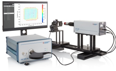
Instrument Systems’ Drs Frank Münchow and Karthik Iyer explain in an upcoming PhotonicsViews article how to minimize the error budget of a VCSEL test system and provide highly accurate measured values for the eye safety of the laser source.
In a two-part tutorial in PhotonicsViews 1 and 2/2022, Joya Team share their experience of more than two decades with the professional community.
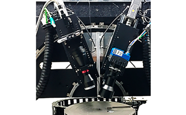
Based on a novel measurement algorithm and the Mikrotron EoSens 12CXP+ area scan camera, scientists in Taiwan developed a system to reconstruct a 3D model in a continuous scan mode instead of the conventional approach of taking three full-field fringe images sequentially in pause mode.