UFO for wafer level testing
Jenoptik provides an essential component for novel PIC wafer level tests with the optoelectronic UFO Probe Card. Users benefit from a fast and simple integration, high flexibility, and state-of-the-art test technology.
In line with an increasing demand for photonic solutions in the semiconductor sector, the requirements for corresponding ecosystems for optoelectronic components are rising and thus, not only semiconductor manufacturers with their own supply chain must change their thinking. In addition to the existing test infrastructure for electrical components, also infrastructures for photonic component testing are required. Test houses offering services such as wafer level testing for fabless manufacturers face the challenge of expanding or reimagine their test solutions towards photonic integrated circuits (PICs).
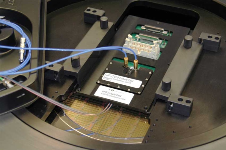
In addition to the established tests for ICs, RoodMicrotec now also offers a test service for this new type of PIC testing at wafer level to customers from the semiconductor industry. Jenoptik provides the necessary technology platform with the UFO Probe Card and thus supports RoodMicrotec in setting up the respective test structure.
The device enables the testing of electrical and optical components with only one probe card – in parallel, not sequentially as with previous solutions. Thus, wafer level tests can be performed in a more time-saving manner and the throughput is significantly increased. As a plug-and-play solution, the hybrid probe card can be integrated directly and without much of an adaption effort into RoodMicrotec’s existing standard IC wafer probers. The existing infrastructure can be used immediately, thus simplifying the conversion of test procedures from the classic probe card for electrical components to the hybrid UFO Probe Card within the manufacturing process.
The device does not require active alignment of the optical interfaces for every single chip. This reduces the test time and cost for each chip and several chips can also be tested in parallel. Thus, the time needed to separate good from bad components is considerably lower if already done during PIC wafer-level testing and the overall yield can be significantly improved, since only functioning chips are transferred to further manufacturing processes. Customers benefit from fewer rejects and thus reduced costs.
“As an innovative technology platform, the UFO Probe Card offers the necessary flexibility and scalability. This enables test service providers like us to respond quickly and easily to new challenges in the market,” says Jan de Koning Gans, managing director of RoodMicrotec.
“We are pleased to have RoodMicrotec as a strong and experienced partner for test services, and as a supply chain specialist and service provider for the semiconductor industry it also has access to a wide range of applications. It is important for Jenoptik to recognize the different needs of the end customers in order to promote relevant further developments at an early stage,” says Tobias Gnausch, product manager for the UFO Probe Card in Jenoptik’s light and optics division.
For the future, both companies plan to create standardizations for wafer-level PIC testing to become even more efficient and cost-effective. With the jointly created solutions, our customers can take the step towards the future and increasingly rely on photonic solutions.