Jena research team receives Thuringian Research Prize
Four scientists from Friedrich Schiller University Jena and the Fraunhofer Institute for Applied Optics and Precision Engineering IOF have been awarded the “Thüringer Forschungspreis”.
A hundred thousand times thinner than a hair, stronger than steel and efficient mediators between light and electricity – so-called 2D materials are a rapidly developing class of materials with unique properties and great application potential.
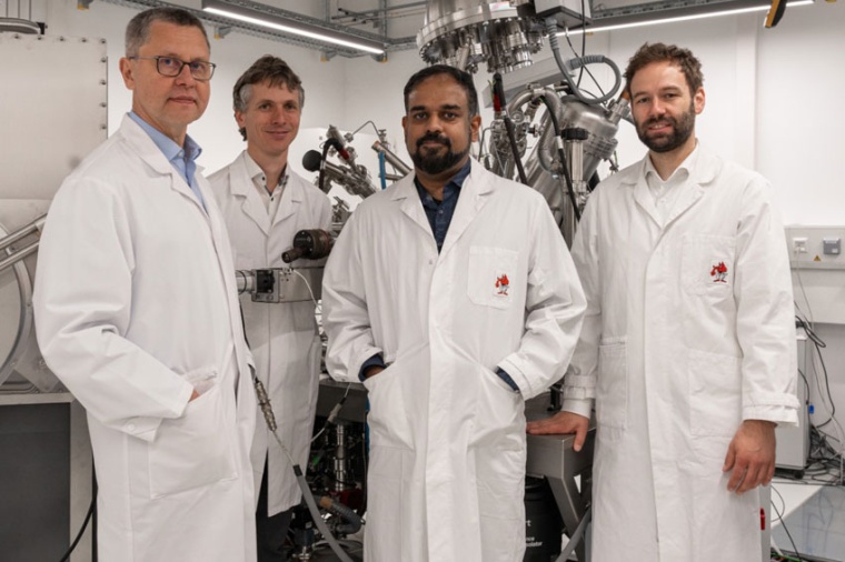
For their research into these 2D materials, researchers from the University of Jena and Fraunhofer IOF have now been awarded the “Thüringer Forschungspreis” (Thuringian Research Prize). The award in the “Applied Research” category, which is endowed with 25,000 euros, was presented on June 18 at the TU Ilmenau. The prize winners – Prof Andrey Turchanin and Drs Antony George, Christof Neumann, and Falk Eilenberger (Fraunhofer IOF) – have developed a range of innovative methods to produce and utilize tailor-made 2D materials for photonic, electronic and optoelectronic applications.
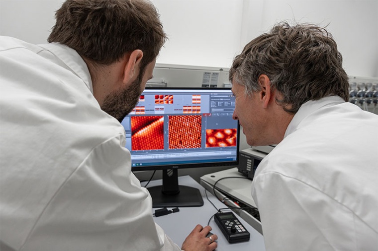
The 2D materials studied represent a new class of materials that consist of just one or a few atomic layers - a hint of nothing. What is special about them: They drastically change their properties compared to the three-dimensional starting materials. One well-known nanomaterial is graphene. A 2D material that is isolated through the deposition of only nanometer-sized layers of graphite. In its atomic form, it is much stronger and more conductive than the starting material graphite, which we know from conventional pencils, for example.
At Fraunhofer IOF, Falk Eilenberger, head of the department of micro and nanostructured optics, has studied and characterized the related material class of transition metal dichalcogenides, or TMDs for short. In their three-dimensional form, TMDs only occur as indirect semiconductors, which limits the potential applications. As a 2D material, however, the substance transforms into a direct semiconductor that can efficiently convert electricity into light and vice versa.
Until now, 2D materials have been obtained by “peeling off” three-dimensional crystals. Similar to peeling off a fingerprint with adhesive tape, individual layers of the crystals are removed piece by piece. This is a time-consuming process that is unsuitable for use in industry and has so far limited the potential applications of the materials.
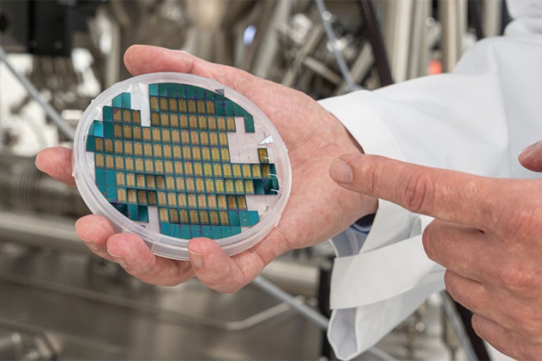
The researchers from Jena have focused on a process that facilitates the industry-compatible production of customized 2D materials. To do this, they use what is known as vapor deposition, in which the crystal grows on a silicon or glass plate like a carpet – a nanometer-thin carpet.
”The new process not only made it possible for us to produce the 2D materials efficiently, but also to grow them scalably as functional parts on optical components,” explains Dr Eilenberger. “This allows us to integrate TMD materials into optical fibers, among other things, which opens up a range of new application possibilities.”
Possibly the world’s smallest LED
By introducing TMD, optical fibers and photonic chips can be functionalized in such a way that they not only passively transmit light, but also generate, change or detect it: an ideal platform, for example, to implement certain tasks of classic computer chips photonically in an energy-saving way in the future. The research team also succeeded in functionalizing the 2D material as a diode and thus developing what is possibly the world’s smallest LED.
The integration of nanomaterials enables electronic, photonic and optoelectronic components to be produced for the first time that are both extremely small and powerful. The efficient conversion of electricity and light also makes the 2D materials interesting for applications in data transmission, camera technology or illumination systems. They can also be seamlessly combined with existing semiconductors, thus opening up new avenues in semiconductor technology.
The resulting light can also have very unusual quantum properties. It is therefore not only suitable for classic data transport, but also for quantum encryption. TMD-loaded optical components can therefore also make a contribution to the quantum security of data communication networks in the future.
Company
Friedrich-Schiller-Universität JenaFürstengraben 1
07743 Jena
Germany
most read
Global robot density: Western Europe leads ahead of North America and Asia
In the EU-27, the robot density is 231, which is above the global average of 132.
Hoerbiger takes over Physik Instrumente
With 1,900 employees, PI will form the new Positioning Division at Hoerbiger as an independent unit.
Steute Technologies buys Kiepe Industry
Steute Technologies, backed by Battery Ventures, has acquired the industrial switching technology specialist and part of Kiepe Electric GmbH

5 robotics trends for 2026
The International Federation of Robotics reports on the five most important trends for the robotics industry in 2026.

Machine Safety 2026: The Five Most Important Trends for Eutomation Engineers
Digitalization and automation continue to drive mechanical engineering forward - and with them, the requirements for functional safety and cyber security are increasing. For automation engineers, this means that machine safety is becoming a holistic concept.


