

In-house rapid prototyping at PTB in Berlin
The lab’s LPKF ProtoLaser U4 processes a wide variety of materials, even HF.
The Physikalisch-Technische Bundesanstalt (PTB), as the National Metrology Institute of Germany, enjoys an excellent reputation throughout the world. For its scientific and metrological development work, it often needs special electronic devices that are not available on the market. The corresponding solutions are designed by the scientists and development engineers at PTB and then manufactured by the department “Nutzerunterstützung” (user support), an internal service provider, as single-sided or double-sided PCBs. For this, the institute uses in-house prototyping equipment from LPKF.
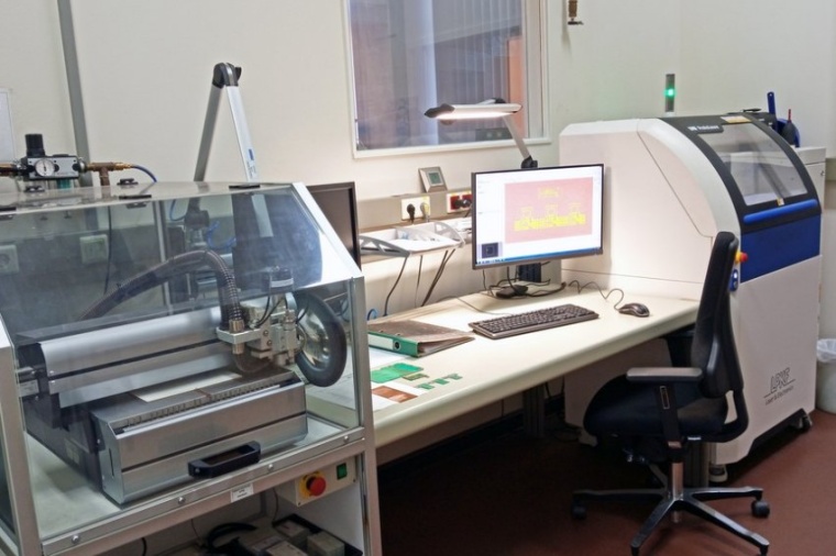
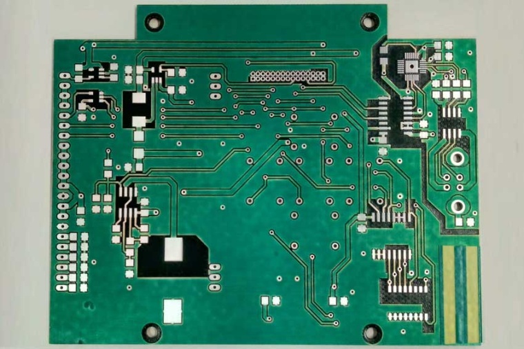
Electronic devices are developed for measuring physical quantities such as pressure, magnetic fields, luminosity, fluid flow, temperature, current, or voltage. They are often combined with application-specific control panels and displays that are based on microcontroller boards or connected to automated measuring stations via different communication modules and protocols such as USB, RS232, RS485, or Ethernet. In some cases, extremely low-noise amplifiers, special power supplies or various other devices are needed as well.
Many projects have to meet a strict timeframe, and the equipment is needed promptly. For rapid manufacturing of the PCB prototypes, the lab has an LPKF ProtoMat H60 circuit board plotter, an LPKF ProtoLaser U4 laser system, and the LPKF Contac S4 through-hole plating system. A process for creating solder masks with LPKF ProMask as well as additional devices such as a programmable oven for drying and curing, a UV exposure unit for polymerization, a measuring device for the PCB copper thickness – including the copper in the vias – and a stereomicroscope are also used in the lab.
Speed is of the essence due to the large number of PCBs produced by the service provider. If drilling and structuring must both be performed by the same machine, the LPKF ProtoLaser U4 is used. This laser system can process a wide variety of materials, even HF materials. That is important because at PTB, many different materials – even new materials – are used. With the lab equipment, employees process, for example, FR4 material with a thickness of 1.0 mm or 1.55 mm and a copper layer of thickness 18 µm or 35 µm or Rogers RO4003 or TMM10i. Flex materials and ceramics can be processed reliably with the ProtoLaser. Processing of aluminum oxide of thickness 1.0 mm with 35 µm copper for applications with higher current intensities and accordingly stronger heat generation also works very well. Demands on processing speed have increased dramatically over the last few years – especially for structures smaller than 100 µm. Through its capacity to drill and structure, the ProtoLaser U4, which is considered an “all-around genius” at PTB, makes it possible to implement the high requirements.
In addition, the lab employees use LPKF ProMask to create solder masks. This makes later assembly easier and reduces, for example, tin requirements for the chemical process of immersion tin coating. The PTB service provider uses an LPKF Contac S4 for through-hole plating. With this new system, through-hole plating of holes smaller than 0.4 mm no longer causes problems.
Incidentally, PTB also has an electronics training center in which apprentices and students can learn all about PCB design. Many of the budding engineers need the PCB service for their final projects. For that, it is extremely helpful to be able to perform prototyping directly and quickly with LPKF’s in-house equipment for PCB manufacturing. (Source: LPKF)
Company
Physikalisch-Technische Bundesanstalt (PTB)Bundesallee 100
38116 Braunschweig
Germany


most read

Siemens Consolidates Its Automation Business into a New Unit Called Automation
Rainer Brehm, who previously served as COO of the automation business and CTO of Digital Industries, was appointed president of the new unit.
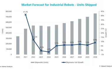
Forecast: Significant Growth in Industrial Robotics by 2030; Cobots Are Growing the Fastest
According to a recent analysis by Interact Analysis, global sales of industrial robots are expected to rise from about 550,000 units in 2025 to just over 760,000 units in 2030.

ZVEI Calls for Swift Protection of Critical Power Infrastructure
The association has issued a statement in response to the recent attempted attacks on substations in Brandenburg and North Rhine-Westphalia and warns of the consequences for Germany's energy security.

European machine vision expects slight recovery and growth in 2026
According to the VDMA Machine Vision department, sales are expected to increase by around 3%, following a decline of 2% in 2025.
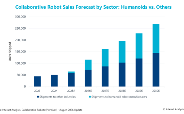
Humanoid robotics is driving demand for cobot arms and actuators
According to recent analyses, global production of humanoid robots exceeded the 20,000-unit mark in 2025 and is expected to more than triple in 2026.