“New technologies always start in R&D”
Kolja Haberland, CTO at Laytec, talks about the early years of the company and explains how they managed to grow from a three-person operation to a globally active medium-sized enterprise
PhotonicsViews: Already in the 90s, you were working on in-situ metrology of III-V materials. How did this lead to the creation of Laytec?
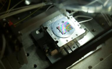
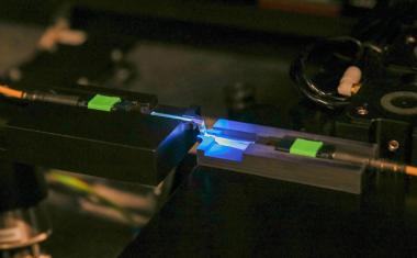
Kolja Haberland: Laytec started in 1998 while I was doing a PhD in Physics at the Technical University of Berlin. I was working on metrology for III-V materials using an optical tool called a reflectance anisotropy spectrometer (RAS), a non-invasive optical instrument we had developed in Berlin that characterizes the optical anisotropy of a surface.
This tool was really useful to understand what is going on inside an MOCVD system during growth of III-V materials like Gallium Arsenide and Indium Phosphide. We published data, went to conferences and attracted a lot of interest because at that time, there were no standard tools for in-siu metrology of III-V epitaxy. Researchers started to ask us to build them an RAS system, so two colleagues and me co-founded Laytec in 1999, and when the company grew, I took the role of CTO.
PhotonicsViews: How has Laytec developed?
Haberland: Initially, we focused on in-situ metrology for thin-film growth epitaxy processes like MOCVD, especially for LEDs and lasers. By the late-2000s we had grown rapidly and we broadened into in-line metrology for large-area deposition techniques for amorphous, polycrystalline, organic thin films as used in photovoltaics (PV) and display industries. Today we are also providing stand-alone wafer mapping systems and in-situ metrology for dry etching processes.
In 2018 we had reached a size and market penetration where we wanted to talk to large semiconductor players in Asia and the US. However, we did not have the capacity to achieve this. With the takeover by the Nynomic Group, we were able to benefit from their experience, expertise, and innovative strength.
We now have a workforce of 70, and an international distribution and service network covering Europe, China, Taiwan, Korea, Japan, Malaysia, North America, and India. Over the last almost 30 years we have installed more than 4,000 metrology systems worldwide.
Continue with login
No account yet?
Register now for free and get full access to all exclusive articles from wileyindustrynews.com.
With our newsletter we regularly send you top news from Automation, image processing and light and laser technology in industrial environments, as well as the latest e-issue.
Company
LayTec AGSeesener Str. 10–13
10709 Berlin
Germany


most read
The Rise of Photonic and Neuromorphic Computing: A New Era for AI Hardware
Computer Architectures for future data processing

Could the global industrial automation market face another supply chain crunch?
In 2025, industrial automation OEMs faced uncertainty due to a US-China trade policy shift, delaying orders.
Systematic Characterization of Ring-Shaped Laser Beams
New metrics for meaningful analysis beyond ISO 11146.
Active Alignment in Assembly and Connection Technology
Reliable manufacturing processes are essential for the assembly and connection technology of photonics systems. Common coupling methods of Active Alignment during assembly are described here.
Chatbots for Dead, Endangered, and Extinct Languages
Possibilities and Limitations of Generative AI for Continuing Education.