Precise Down to the Nanometer
Interferometry is crucial in semiconductor, packaging, and medical industries. New white‑light systems offer nanometer precision, high measurement rates, and are ideal for inline industrial use
Alexander Streicher, Product Manager Sensors at Micro-Epsilon
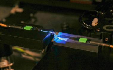
White light interferometers use interference effects of polychromatic light, which consists of many different wavelengths, to obtain information about the distance to a surface or the thickness of an object. The light source emits a continuous spectrum of light waves, which is divided into a reference beam and a measurement beam. The two reflected beams meet and overlap. By varying the phase shift with the wavelength, constructive interference occurs at certain wavelengths and destructive interference at others.
If the intensity of this interference signal is plotted against the wavelength, alternating minima and maxima appear. The resulting periodic intensity signal in the spectrum of the reflected light is assigned to a distance or a thickness by means of Fourier transformation. In a thickness measurement, the two beams that are reflected from the front and back of the coating interfere with each other. This means that the measurement result is also independent of the distance to the measuring object.
Differences Compared to Laser Interferometers
In contrast to laser interferometers, Micro-Epsilon white light interferometers work with polychromatic white light and an extended wavelength spectrum. This means that significantly more information is available for evaluating the superposition of received wavelengths. This results in a number of advantages, including:
- absolute distance measurement without referencing,
- thickness measurements with maximum precision and signal stability, even with fluttering objects,
- wide range of applications such as distance, multi-layer or thickness measurements,
- maximum signal stability for industry, semiconductors, mechanical engineering or laboratories.
Infinitely Adjustable Measuring Rate
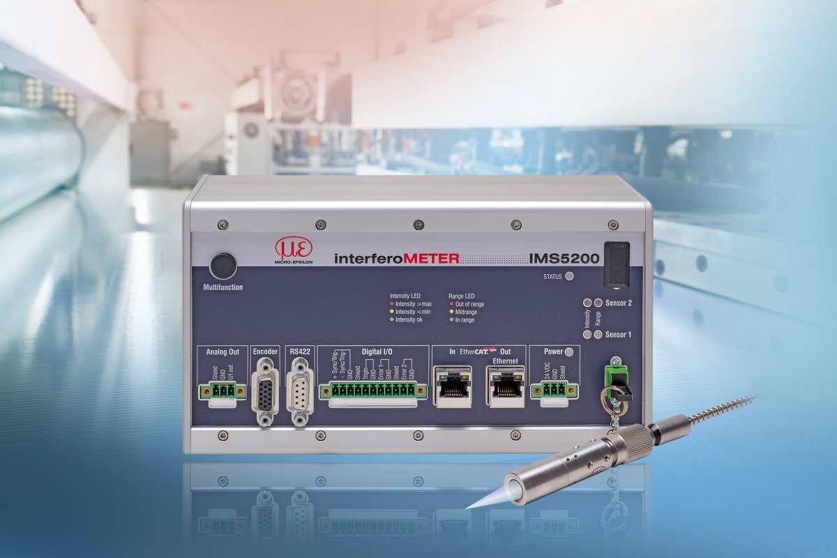
The new interferometer series IMS5200 is characterized by a continuously adjustable measuring rate from 100 Hz to 24 kHz, an excellent linearity of ± 100 nm and the possibility to measure very thin transparent layers. Users can also perform multi-peak thickness measurements with up to five layers. Due to advanced algorithms, Micro-Epsilon interferometers also measure very precisely within a large operating range of ± 2 mm.
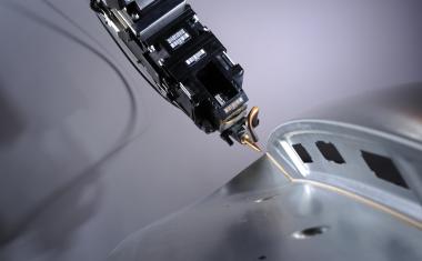
The passively cooled metal housing of the controller is designed to IP40 and can be mounted on the DIN rail in the control cabinet. The sensor can also be installed in a vacuum, which has many advantages for the semiconductor industry in particular. Micro-Epsilon offers a comprehensive range of cleaned and cleanroom-packed accessories for easy integration of the measuring system into vacuum environments. Fiber optic cables of up to 10 m also allow the sensor and electronics to be physically separated to keep high temperatures away from the controller.
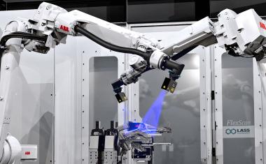
The sensor and controller unit are already preconfigured at the factory for easy commissioning. The controllers can be integrated into modern networks via interfaces such as Ethernet, Ethercat, Profinet or RS422 and have encoder connections and digital I/Os. Due to the versatile interfaces, the acquired measurement values can be processed efficiently via existing digital and analog outputs. Integration into existing automation systems such as programmable logic controllers is also not a problem.
Convenient Installation and Configuration
Interferometers of the IMS5200 series provide absolute measurement values in contrast to conventional laser interferometers that use relative measurements. As a result, they provide stable and absolute measurements without prior referencing. This is particularly advantageous in the event of signal interruptions, which can be caused by false reflections, for example. After the signal interruption, users immediately receive a measured value, whereas laser interferometers first have to re-reference themselves. This allows distance profiles of moving measuring objects to be generated with high precision and reliability.
The entire configuration of the interferometers can be carried out via an intuitive web interface and without additional software. To do so, the user calls up the web interface via an Ethernet connection on the PC and can then set parameters such as messages, measuring rate or number of layers. An editable materials table is available especially for thickness measurement. Ready-made presets for various measurement tasks simplify commissioning and lead to quick results.
Easy Replacement
The sensor's visible measuring point, which visualizes the measuring position, ensures high-precision measurements. The modular design in particular makes it easier to replace and calibrate the sensors. The components can be replaced quickly and easily, allowing users to react to possible failures at any time. Light sources can also be replaced by the manufacturer's service team. If you want to replace the sensor with a sensor of the same type, there is no need to remove the sensor or recalibrate it at the factory. It is also possible to adjust the cable length and replace it with cables of the same type.
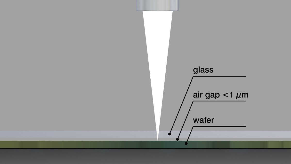
Example from the Semiconductor Industry
One of the many applications of the interferometer IMS5200 is measuring the air gap of glass wafers and masks in semiconductor production. Here, the polychromatic light is directed vertically onto the glass and wafer. Part of the light is reflected on the underside of the glass, another part on the wafer. Between them is an air gap with a thickness of several µm. The two light beams overlap and create an interference pattern that depends on the slit size. This enables non-contact detection of whether the wafer is correctly positioned or whether the optimum distance between the mask and wafer for the process is being maintained. With this measuring method, the company increases the quality of products in the semiconductor industry.
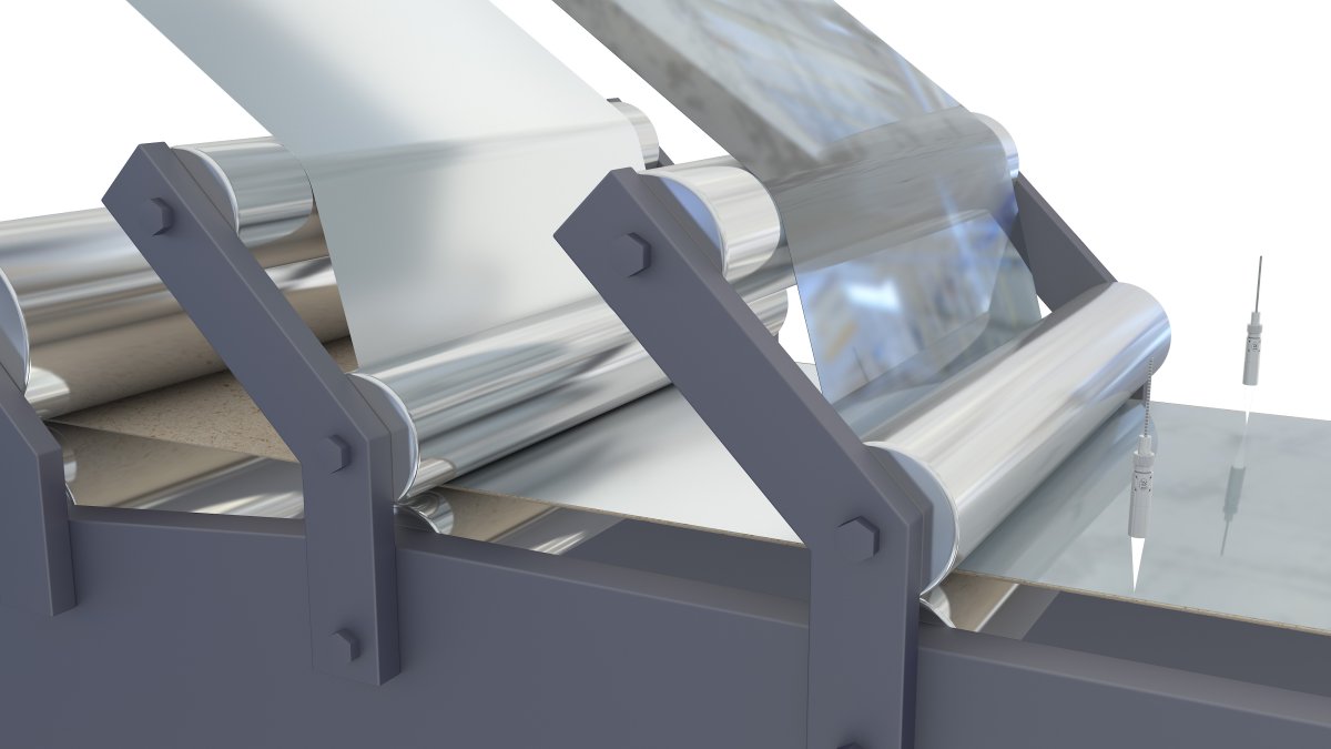
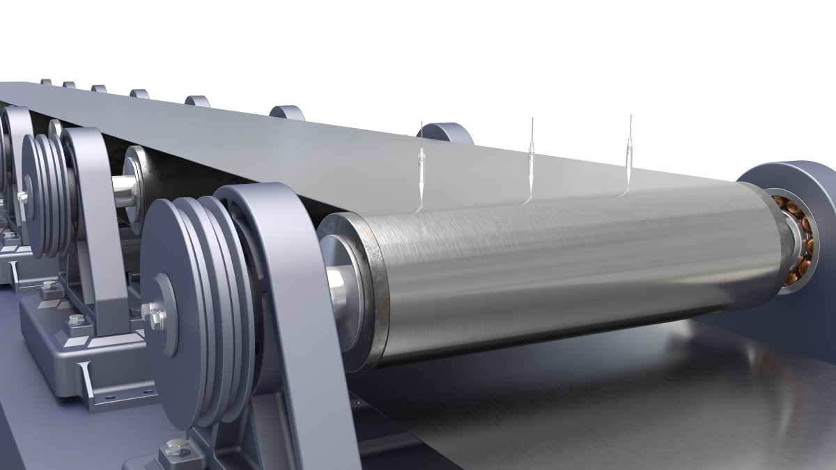
Inspecting Beverage Cartons
The IMS5200 is also used in the packaging industry. For example, the white light interferometer tests the coating of beverage cartons by emitting broadband light onto the surface and evaluating the reflected signals of the layer boundaries. From this, the thickness of the coating can be derived precisely and without contact. This allows defective areas, uneven layers or air pockets in beverage cartons to be detected at an early stage and rejects are avoided.
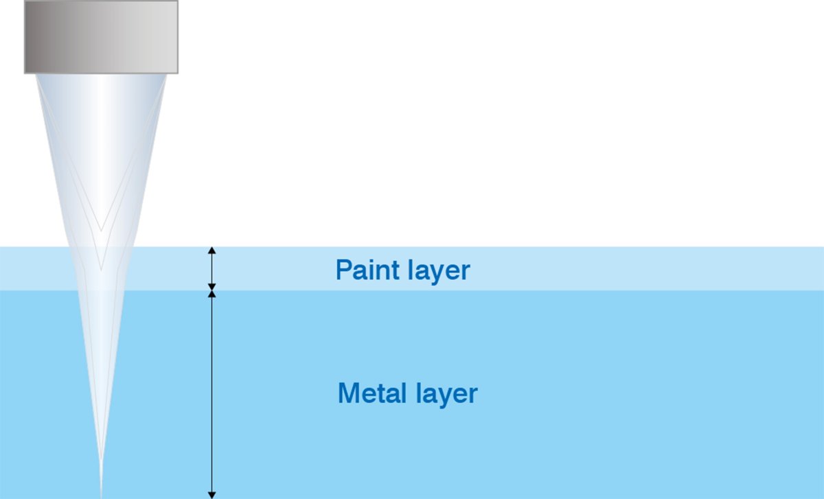
Paint Thickness Testing in the Metal Industry
Testing the paint thickness is another application. Here, the white light interferometer emits broadband light onto the painted metal surface and measures the interference between the reflections on the paint surface and the underlying metal layer. The exact paint thickness is determined from the distance between the signals, even with very thin, transparent or reflective coatings. This allows the paint density to be checked inline and non-destructively to ensure consistent paint quality.
Conclusion
Micro-Epsilon white light interferometers provide high-precision, non-contact measurement signals for determining distances, layer thicknesses and surface structures with nanometer resolution. They are ideal for transparent, reflective or multi-layered materials and provide absolute measurement values in industrial applications. They are accurate, can be used flexibly and are inline-capable, which makes them particularly valuable in the semiconductor and packaging industries.