Optimized 3D-printing of optically active nanostructures
The shape, size and optical properties of three-dimensional nanostructures can now be simulated in advance before they are produced directly with high precision on a wide variety of surfaces.
For around twenty years, it has been possible to modify surfaces via nanoparticles so that they concentrate or manipulate light in the desired way or trigger other reactions. Such optically active nanostructures can be found in solar cells and biological or chemical sensors, for example. In order to expand their range of applications, researchers at the Institute of Electron Microscopy and Nanoanalysis (Graz University of Technology) and the Graz Center of Electron Microscopy (ZFE) have been working for more than one decade on manufacturing not only flat nanostructures, but in particular complex, free-standing 3D architectures.
The team led by Harald Plank, Verena Reisecker and David Kuhness has achieved two breakthroughs. It is now possible to precisely simulate the required shapes and sizes of nanostructures in advance to achieve the desired optical properties, which can then be accurately produced. They have also managed to completely remove chemical impurities, incorporated during initial production without negatively impacting the 3D nanoarchitectures.
Until now, three-dimensional nanostructures required a time consuming trial-and-error process until the product revealed the desired optical properties. This effort has finally been eliminated. “The consistency between simulations and real plasmonic resonances of a wide range of nanoarchitectures is very high,” explains Plank. “This is a huge step forward. The hard work of the last few years has finally paid off.” The technology is currently the only one in the world that can be used to produce complex three-dimensional structures with individual features smaller than ten nanometers in a controlled, single step procedure on almost any surface. “The biggest challenge in recent years was to transfer the 3D architectures into high-purity materials without destroying the morphology,” adds Plank. “This development leap enables new optical effects and application concepts thanks to the 3D aspect.” Nanoprobes or optical tweezers with sizes in the nanometer range are now within reach.
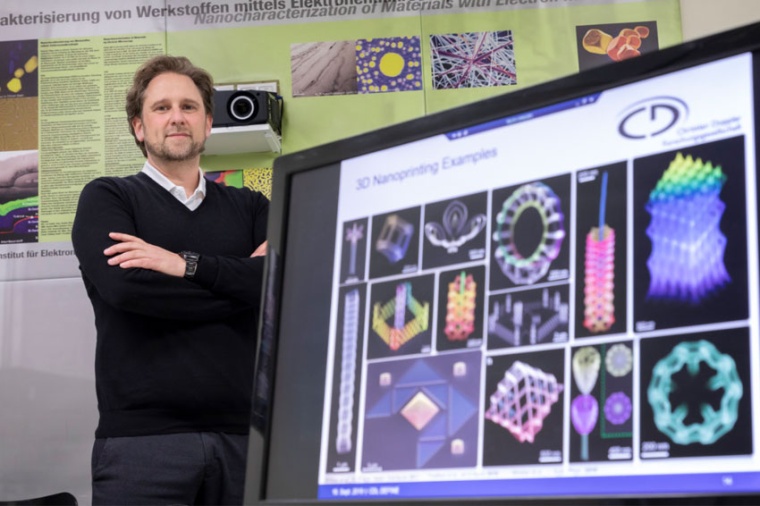
The researchers use focused electron beam induced deposition to produce the nanostructures. The relevant surface is exposed to special gases under vacuum conditions. A finely focused electron beam splits the gas molecules, whereupon parts of them change into a solid state and adhere to the desired location. “By precisely controlling beam movements and exposure times, we are able to produce complex nanostructures with lattice or sheet-like building blocks in a single step”, explains Harald Plank. By stacking these nano-volumes on top of each other, three-dimensional structures can ultimately be constructed. (Source: TU Graz)
Reference: V. Reisecker et al.: Spectral Tuning of Plasmonic Activity in 3D Nanostructures via High-Precision Nano-Printing, Adv. Funct. Mater.; DOI: 10.1002/adfm.202310110