Zeiss Strengthens Its Semiconductor Business with a New Semiconductor Innovation Center in Korea
The center brings together systems from the Semiconductor Fab Solutions and Semiconductor Mask Solutions divisions and serves high-volume wafer production, wafer-level packaging, and photomask manufacturing.
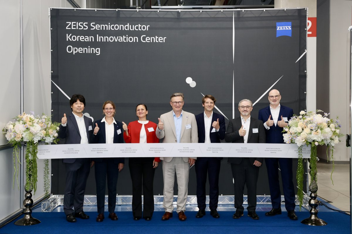
Zeiss Semiconductor Manufacturing Technology has opened a Semiconductor Innovation Center in Yongin, Korea, which serves as a local hub for collaboration with Korean chip and mask manufacturers. The center brings together systems from the Semiconductor Fab Solutions and Semiconductor Mask Solutions divisions and addresses high-volume wafer production, wafer-level packaging, and photomask manufacturing.
Among the systems installed are the nlx-100 for 3D X-ray metrology and inspection of complex package structures, the dune100 for active wafer shape control with integrated precision measurement technology, and the Merit AE—the next generation of mask repair technology for very small defects on photomasks. These systems support process control, yield optimization, and faster evaluation in real production environments.
The center facilitates joint development, process optimization, and accelerated qualification, and is intended to facilitate the integration of new technologies into Korean fabs. Zeiss plans to further expand its portfolio on site.