Nanoscale lattices flow from 3D printer
Lasers write the lines by prompting the ink to absorb two photons, initiating free-radical polymerization of the material.
Weaving intricate, microscopic patterns of crystal or glass is now possible thanks to engineers at Rice University. The materials scientists are creating nanostructures of silica with a sophisticated 3D printer, demonstrating a method to make microscale electronic, mechanical and photonic devices from the bottom up. The products can be doped and their crystal structures tuned for various applications.
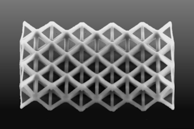
The electronics industry is built upon silicon, the basic semiconducting substrate for microprocessors for decades. The study addresses the limitations of top-down manufacturing by turning the process on its head. “It’s very tough to make complicated, three-dimensional geometries with traditional photolithography techniques,” Jun Lou, a professor of materials science and nanoengineering, said. “It’s also not very ‘green’ because it requires a lot of chemicals and a lot of steps. And even with all that effort, some structures are impossible to make with those methods. “In principle, we can print arbitrary 3D shapes, which could be very interesting for making exotic photonic devices,” he said. “That’s what we’re trying to demonstrate.”
The lab uses a two-photon polymerization process to print structures with lines only several hundred nanometers wide. Lasers write the lines by prompting the ink to absorb two photons, initiating free-radical polymerization of the material. “Normal polymerization involves polymer monomers and photoinitiators, molecules that absorb light and generate free radicals,” said graduate student Boyu Zhang of the process that commonly uses ultraviolet light in 3D printing and to cure coatings and in dental applications.
“In our process, the photoinitiators absorb two photons at the same time, which requires a lot of energy,” he said. “Only a very small peak of this energy causes polymerization, and that in only a very tiny space. That’s why this process allows us to go beyond the diffraction limit of light.” The printing process required to develop a unique ink. Zhang and Xiewen Wen, a Rice alumnus, created resins containing nanospheres of silicon dioxide doped with polyethylene glycol to make them soluble.
After printing, the structure is solidified through high-temperature sintering, which eliminates all the polymer from the product, leaving amorphous glass or polycrystalline cristobalite. “When heated, the material goes through phases from glass to crystal, and the higher the temperature, the more ordered the crystals become,” Lou said. The lab also demonstrated doping the material with various rare earth salts to make the products photoluminescent, an important property for optical applications. The lab’s next goal is to refine the process to achieve sub-10 nanometer resolution. (Source: Rice U.)
Link: Dept. of Materials Science and NanoEngineering, Rice University, Houston, USA