Lithography-free photonic chip offers high speed and accuracy
New photonic device provides programmable on-chip information processing for AI applications.
Photonics and electronics draw on separate areas of science and use distinct architectural structures. Both, however, rely on lithography to define their circuit elements and connect them sequentially. While photonic chips don’t make use of the transistors that populate electronic chips’ ever-shrinking and increasingly layered grooves, their complex lithographic patterning guides laser beams through a coherent circuit to form a photonic network that can perform computational algorithms. But now, for the first time, researchers at the University of Pennsylvania School of Engineering and Applied Science have created a photonic device that provides programmable on-chip information processing without lithography, offering the speed of photonics augmented by superior accuracy and flexibility for AI applications.
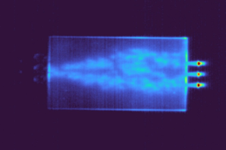
Achieving unparalleled control of light, this device consists of spatially distributed optical gain and loss. Lasers cast light directly on a semiconductor wafer, without the need for defined lithographic pathways. Liang Feng, Tianwei Wu, Zihe Gao and Marco Menarini developed the new microchip. “But photonic chips intended for machine learning applications face the obstacles of an intricate fabrication process where lithographic patterning is fixed, limited in reprogrammability, subject to error or damage and expensive,” says Feng. “By removing the need for lithography, we are creating a new paradigm. Our chip overcomes those obstacles and offers improved accuracy and ultimate reconfigurability given the elimination of all kinds of constraints from predefined features.”
Without lithography, these chips become adaptable data-processing powerhouses. Because patterns are not pre-defined and etched in, the device is intrinsically free of defects. Perhaps more impressively, the lack of lithography renders the microchip impressively reprogrammable, able to tailor its laser-cast patterns for optimal performance, be the task simple (few inputs, small datasets) or complex (many inputs, large datasets). In other words, the intricacy or minimalism of the device is a sort of living thing, adaptable in ways no etched microchip could be. “What we have here is something incredibly simple,” says Wu. “We can build and use it very quickly. We can integrate it easily with classical electronics. And we can reprogram it, changing the laser patterns on the fly to achieve real-time reconfigurable computing for on-chip training of an AI network.”
An unassuming slab of semiconductor, the device couldn’t be simpler. It’s the manipulation of this slab’s material properties that is the key to research team’s breakthrough in projecting lasers into dynamically programmable patterns to reconfigure the computing functions of the photonic information processor. This ultimate reconfigurability is critical for real-time machine learning and AI. “The interesting part,” says Menarini, “is how we are controlling the light. Conventional photonic chips are technologies based on passive material, meaning its material scatters light, bouncing it back and forth. Our material is active. The beam of pumping light modifies the material such that when the signal beam arrives, it can release energy and increase the amplitude of signals.”
“This active nature is the key to this science, and the solution required to achieve our lithography-free technology,” adds Gao. “We can use it to reroute optical signals and program optical information processing on-chip.” Feng compares the technology to an artistic tool, a pen for drawing pictures on a blank page. “What we have achieved is exactly the same: pumping light is our pen to draw the photonic computational network on a piece of unpatterned semiconductor wafer.” But unlike indelible lines of ink, these beams of light can be drawn and redrawn, their patterns tracing innumerable paths to the future. (Source: UPenn)