

Laser system for producing high purity crystals
Researchers from Japan and Germany have now developed a method to produce semiconductor crystals for power electronics using a laser-based process.
In modern electrical engineering, relatively high power must be switched quickly. To accomplish this, the electronics are based on wide-bandgap semiconductors such as gallium oxide (Ga2O3). Since it has a melting point of around 1,800 °C and is grown from the melt, this material is easier to produce than other wide-bandgap semiconductors such as silicon carbide (SiC) or gallium nitride (GaN), both of which are grown using chemical vapor deposition. To date, crucible-based methods such as the Czochralski and the edge-defined film-fed growth (EFG) processes have mainly been used to produce gallium oxide crystals. However, the purity of the crystal is limited by the diffusion of the crucible material.
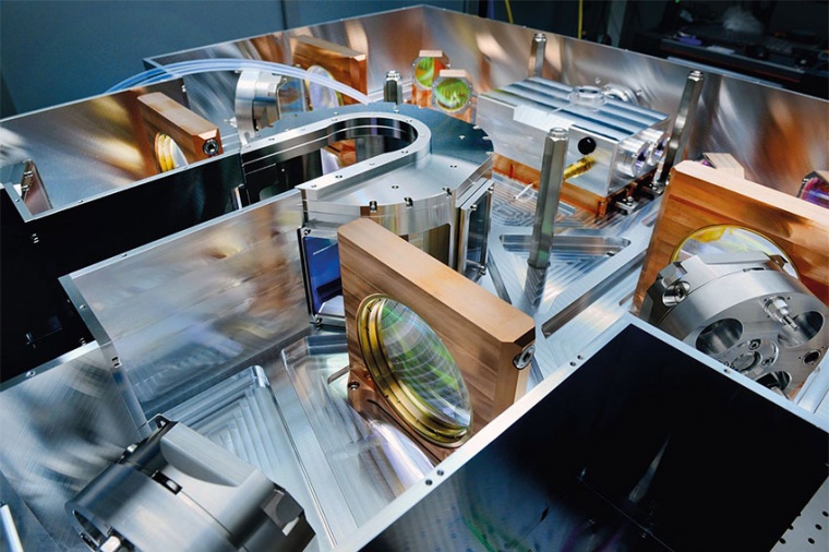
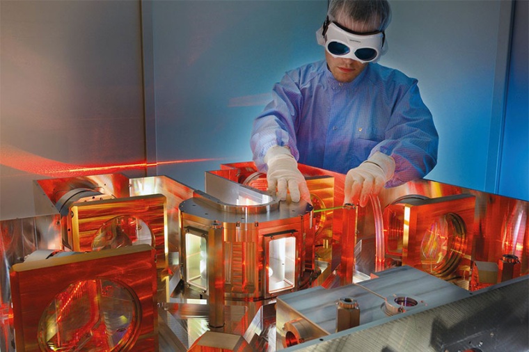
Contamination of the melt can be avoided by supplying the heat in the form of radiation, rather than via the crucible, which causes the polycrystalline starting material to be remelted into a high-purity single crystal. Of course, this can also be achieved with heating lamps. In contrast to heating lamps, however, the emission of the laser not only has long term stability, but the laser also only emits its radiation in one direction, which means that the heat input is much more targeted. In addition, the laser beam profile can be optimized with regard to the heating process. The possible crystal diameters scale with the heating power, so that increasingly powerful laser systems have been used for the laser-diode floating zone (LDFZ) process in recent years.
Using laser powers of more than 5 kW for growing crystals is new; until now, comparable powers have been used in established laser material processing methods such as cutting and welding. The optical systems for this have to be designed and cooled carefully, as even small losses of less than one percent can lead to their destruction during prolonged use. Fraunhofer ILT in Aachen has, therefore, developed a water-cooled high-performance optical system especially for the LDFZ process. With it, the radiation emitted by the laser is initially split into five partial beams with a maximum of 4 kW each. The partial beams are then deflected via large, water-cooled mirrors in such a way that they heat the crystal in the center of the setup evenly, offset by exactly 72 degrees.
The optics were set up and characterized in Aachen and then transferred to the project partners in Japan. They were installed in compliance with pandemic regulations, and Aachen project manager Dr Martin Traub is satisfied: “Commissioning via video conference was a real novelty, but it worked well. The test phase was successful and the system was operated reliably until the planned end of the project.”
Project partner Dr Toshimitsu Ito from the National Institute of Advanced Industrial Science and Technology (AIST) in Tsukuba Science City in Japan has already gained a great deal of experience with the LDFZ process. The institute was able to produce gallium oxide crystals with a diameter of up to 12 mm at lower laser powers. With the new 20 kW system, it should be possible to significantly increase the diameter. After commissioning and initial tests to melt the gallium oxide raw material, AIST carried out crystal growth experiments with the new LDFZ system. The results of these investigations will be published shortly, but this much can already be said: The project partners succeeded in growing crystals with a diameter of up to 30 mm – the largest gallium oxide crystals ever produced using a crucible-free growth process.
The project was funded by both Japan and Germany. The Fraunhofer-Gesellschaft supports the establishment of long-term partnerships with excellent research institutes abroad in a program for “International Cooperation and Networking”, or ICON for short.
In the future, the partners will investigate how suitable the process is for producing other metal oxides. As part of the BMBF-funded HIPEQ research project, for example, the process will be used to produce optical crystals.
Company
Fraunhofer Institute for Laser Technology ILTSteinbachstr. 15
52074 Aachen
Germany



most read

ZVEI Calls for Swift Protection of Critical Power Infrastructure
The association has issued a statement in response to the recent attempted attacks on substations in Brandenburg and North Rhine-Westphalia and warns of the consequences for Germany's energy security.

European machine vision expects slight recovery and growth in 2026
According to the VDMA Machine Vision department, sales are expected to increase by around 3%, following a decline of 2% in 2025.

Siemens Consolidates Its Automation Business into a New Unit Called Automation
Rainer Brehm, who previously served as COO of the automation business and CTO of Digital Industries, was appointed president of the new unit.

IMTS 2026: America's Manufacturing Sector Focuses on Growth and Technology
The largest manufacturing trade show in the Western Hemisphere is bringing together 1,788 exhibitors this year, including about 400 companies participating for the first time.

Schaeffler bundles Defense and New Space activities under new CEO
Celia Pelaz takes over the position of CEO Defence & New Space at Schaeffler on October 1, 2026 and becomes Chairwoman of the Management Board of Stech Defence GmbH.