Hyperspectral nanoimaging of 2D materials
New imaging technique provides link to innovative products.
When we think about the links to the future - the global transition to solar and wind energy, tactile virtual reality or synthetic neurons - there's no shortage of big ideas. It's the materials to execute the big ideas - the ability to manufacture the lithium-ion batteries, opto-electronics and hydrogen fuel cells - that stand between concept and reality. Enter two-dimensional materials, the latest step in innovation. Consisting of a single layer of atoms, two-dimensional materials like graphene and phosphorene exhibit new properties with far-reaching potential. With a capability to be combined like Lego bricks, these materials offer connections to future products, including new means to convey both power and people, with more-efficient energy transmission, and solar- and wind-powered vehicles on roads and in skies.
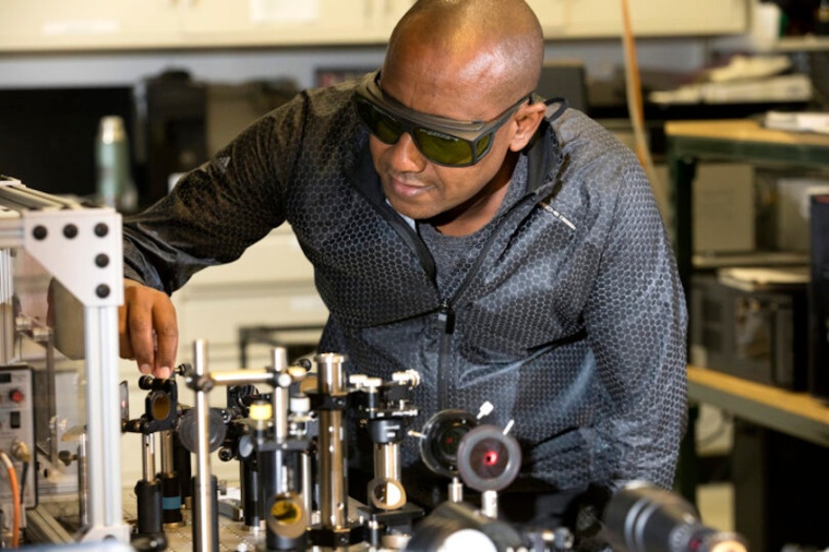
A study led by University of Georgia researchers announces the successful use of a new nanoimaging technique that will allow researchers to test and identify these materials in a comprehensive way at the nanoscale for the first time. Now, there's a way to experiment with new materials for our big ideas at a really, really small scale. “Fundamental science – small-scale electrical conductivity, light emission, structural changes – happen at the nanoscale,” said Yohannes Abate, Susan Dasher and Charles Dasher MD Professor of Physics in the Franklin College of Arts and Sciences. “This new tool allows us to visualize all of this combined at unprecedented specificity and resolution.”
“Since we cannot see atoms with traditional methods, we needed to invent new tools to visualize them,” he said. The hyperspectral imaging technique allows scientists to inspect electrical properties, optical properties, and the mechanical properties at the fundamental length scale, simultaneously. The researchers created a one-atom thick sheet of two kinds of semiconductors stitched together, similar to assembling an atomic Lego, with properties not found in traditional thick materials. With single-atom-thick crystals, each atom is literally exposed on the surface, combining atomic properties that result in new properties.
“At the heart of materials science is the need to understand fundamental properties of new materials, otherwise it is impossible to take advantage of their unique properties,” Abate said. “This technique puts us one step closer to being able to use these materials for a number of potential applications.” Those include various forms of electronics or light-emitting systems applications. How to verify the effect of very small changes in atomic composition, conductivity and light response of single-atom-thick materials simultaneously has been the challenge until now, Abate said.
Nobel Prize-winning physicist Richard Feynman, who envisioned nanotechnology as early as the 1960s, predicted that as scientists became able to choose and replace certain kinds of atoms, they would able to fabricate practically any imaginable material. “More than half a century later, we're not there yet, but where we are, we can visualize them, and at that scale there are new issues that can arise and we have to understand those properties as a part of understanding the large scale material properties, before we can use them,” Abate said. (Source: UGA)
Link: Dept. of Physics and Astronomy, University of Georgia, Athens, USA