Fraunhofer IPMS now offers ultra-trace element analysis on wafers
The Fraunhofer Institute for Photonic Microsystems IPMS is expanding its range of analyses for monitoring wafer contamination
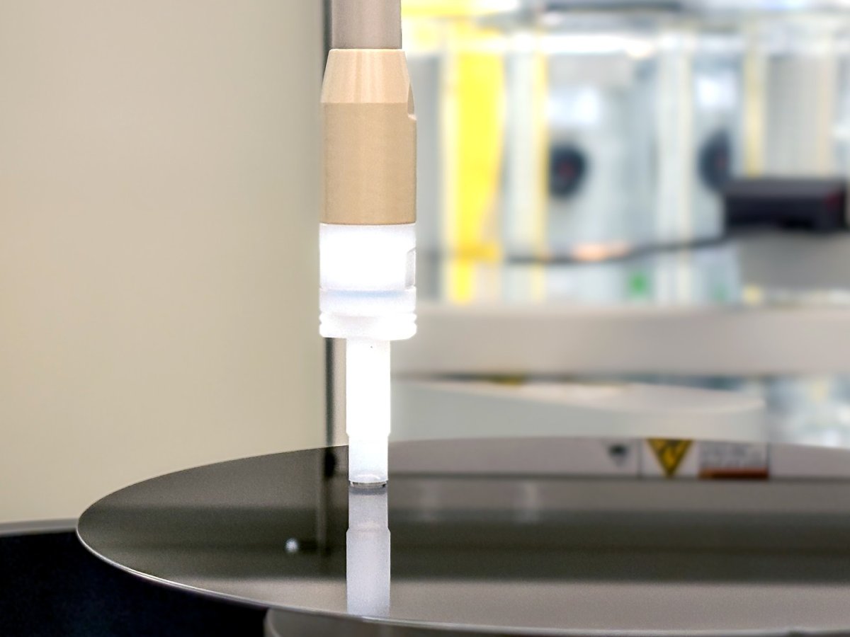
In a new special laboratory, the combination of vapor phase decomposition (VPD) and ICP mass spectrometry (VPD-ICP-MS) is used to quantitatively detect impurities on 200 and 300 mm wafers in the ultra-trace range.
After etching the wafer surface with HF vapor, a drop of scan solution is passed over the surface, collects soluble residues and is then filled up to 1 ml. The analysis by ICP-MS provides highly sensitive, quantitative data on the dissolved elements. As standard, surface and bevel scans for 39 elements are carried out with HF scan solution; for special applications, aqua regia is available as a scan solution for the determination of five precious metals.
The laboratory is equipped with the Wafer Surface Preparation System WSPS2 from PVA Tepla and the iCap RQ mass spectrometer from Thermo Scientific. Fraunhofer IPMS is thus strengthening its role as a leading research institute for 300 mm wafer processing and supporting quality assurance in semiconductor production.