Beginning to see the light
A new early view article in PhotonicsViews presents a rigorous far-field model that allows to calculate the reflectance of the via.
The reflectance of a semiconductor wafer changes if vias or trenches are etched into the semiconductor. We present a rigorous far-field model that allows to calculate the reflectance under consideration of the geometrical properties of the via as well as possible transparent coatings on the wafer surface or transparent fillings in the via. For this the wafer is divided into units with a single via or trench. Each unit can further be divided into regions, the wafer surface region and the via or trench region. Transparent coatings or transparent fillings of the via are considered by simulating the reflectance of each region as the reflectance of a layer stack.
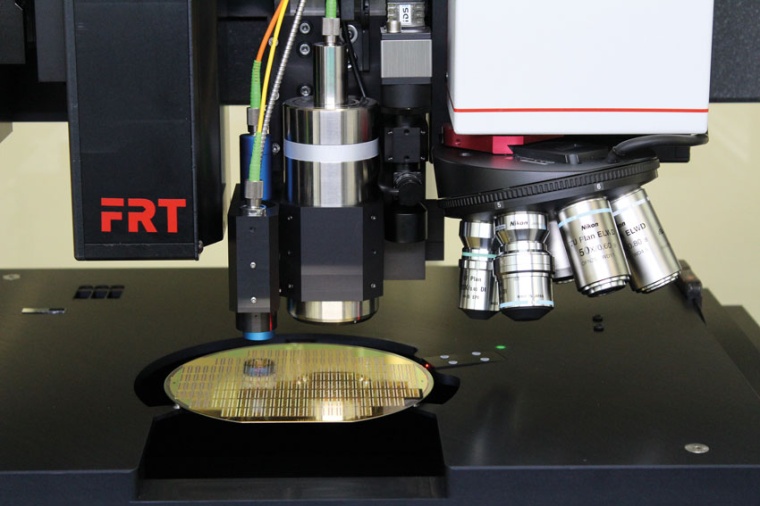
The proposed rigorous model in the far-field is originally intended to be applied on semiconductor surfaces with vias to simulate broadband reflectance spectra of such structured surfaces. The main component of the model is the simulation of the reflectance of each region by the reflectance of a layer stack. By this way, we obtain a large variety of similar structured surfaces, since only thickness of the layers and their refractive indices are necessary to calculate the reflectance of each region. The effects caused by diffraction, scattering, inclined walls, or a curved via bottom are the same also for other materials.
Dr. Quinten Wissenschaftlich-technische Software
Dr. rer. nat. habil. Michael Quinten
52457 Aldenhoven, Germany
phone: +49 2464 2649
e-mail: ulmi.quinten@dn-connect.de
Download: M. Quinten: Beginning to see the light – Calculating the reflectance of semiconductors with vias, PhotonicsViews, E-Special 1, 2025, first published 13 January 2025


