Active Alignment in Assembly and Connection Technology
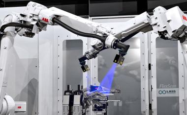
Reliable manufacturing processes are essential for the assembly and connection technology of photonics and optoelectronics systems. One company uses Active Alignment during assembly—a method in which the actual maximum light coupling performance is achieved. The most common coupling methods are described here.
Fiber‑optic communication enables encrypted data transmission in civilian, industrial, and military environments. Lidar systems provide highly accurate environmental sensing in autonomous vehicles. Photonics is also indispensable in aerospace, medical technology, and quantum technology for enabling new applications. Optical sensing, laser‑based distance measurement, or optical neural networks for AI‑driven systems require not only high technological standards but also reliable manufacturing processes.
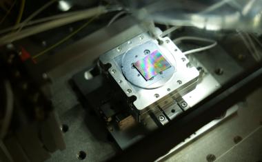
A key element in these processes is the so‑called active‑alignment technology. Unlike passive alignment, where components are positioned according to geometric features, active alignment relies on signal feedback during assembly. This means the process does not just target the geometric center but instead aligns to the actual maximum optical coupling point. Such precision is essential in applications using single‑mode fibers or silicon photonics systems, where even minimal deviations can lead to losses. Hybrid modules with multiple optical interfaces and non‑standard geometries also benefit from this alignment strategy. Tresky Automation combines nanometer‑level accuracy with flexible assembly methods across various coupling processes.
1) Edge Coupling
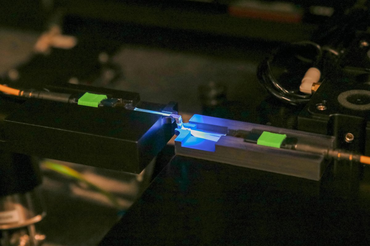
Edge coupling is a method in which light is injected directly into the laterally exposed waveguide of a chip. The optical connection is made via the cleaved facet—a polished or cut edge of the photonic component. This method enables particularly low‑loss coupling, typically with coupling efficiencies of less than 1 dB, making it ideal for demanding high‑performance applications such as silicon photonics (SiPh), laser modules, or high‑speed optical links.
Because edge coupling requires extremely precise alignment—especially when using single‑mode or polarization‑maintaining fibers—active alignment is essential. Only continuous signal monitoring combined with high‑resolution positioning can compensate for unavoidable component tolerances. Coupling signal evaluation with precision mechanics allows maximization of the optical signal and highly reliable assembly at the nanometer scale.
2) Grating Coupling
Another process is grating coupling, also called surface coupling. It is an established optical‑coupling method in which light is coupled vertically—not laterally—into a chip’s waveguide via surface‑structured gratings. Light is typically directed at the grating through fibers positioned at a defined angle, usually between six and ten degrees.
This approach offers larger vertical‑alignment tolerances (Z‑direction) and is therefore particularly suitable for wafer‑level testing or compact optoelectronic modules where space and flexibility are key. Although the coupling efficiency is somewhat lower than with edge coupling—typically around 3-5 dB loss—grating coupling provides major advantages in process integration due to its simpler handling and adjustability, especially for photonics‑chip characterization or modular sensor systems. In automated production, the method can be efficiently combined with active alignment to ensure stable and reproducible optical paths.
3) Lensed‑Fiber, Lens‑Coupling, and Free‑Space‑Coupling Methods
Other coupling methods include lensed‑fiber coupling, lens coupling, and free‑space coupling. These approaches create optical links between components without direct physical contact. They are used when traditional methods such as edge or grating coupling reach their limits.
Light is focused using special lenses—such as spherical, cylindrical, or aspherical micro‑optics—to transfer it across an air gap into the waveguide or onto the optical target with minimal loss. Frequently, lensed fibers are used, with the lens integrated directly into the fiber end, or external lens systems that provide additional alignment degrees of freedom.
This type of coupling offers high flexibility and mechanical decoupling. Because no physical contact occurs between the fiber and chip, it is well suited for applications requiring cleanliness, vacuum compatibility, or long‑term stability—for example in space applications, high‑power laser modules, or hybrid opto‑mechanical systems. The method also allows precise optimization of the beam path via active alignment, including angular and distance correction—particularly advantageous for complex, multi‑channel, or non‑standard geometries.
4) Free‑Space Coupling
Free‑space coupling places particularly high demands on the system’s optomechanical stability, as even the smallest positional changes can degrade alignment. However, with suitable machine technology—such as that provided by Tresky Automation—precise and reproducible coupling can be achieved. This method is ideal for demanding applications in research, defense, medical technology, or quantum optics.
5) Loop Coupling
Loop coupling—also known as ring or resonator coupling—is used to control and distribute optical signals within waveguide‑based systems. Light is guided through a closed optical structure, typically a micro‑ring or micro‑loop, where part of the light is coupled into adjacent waveguides.
This allows precise control of resonance behavior, wavelength filtering, and signal modulation. Loop coupling is widely used in photonics for compact optical filters, wavelength‑division multiplexers (WDM), and sensors. By adjusting coupling strength and loop geometry, bandwidth, Q‑factor, and sensitivity can be finely tuned. This enables high‑density, low‑loss, and customizable photonic integration—an essential building block for modern communications, lidar, and sensing systems.
6) Fiber Coupling
Fiber coupling—also called direct coupling—involves coupling light from a source, such as a laser diode or VCSEL, directly into an optical fiber without intermediate lenses. This interface is fundamental in photonics, as it enables efficient transmission of optical signals between components, modules, or entire systems.
High coupling efficiency depends on precise alignment, nanometer‑scale positioning, and thermal and mechanical stability. Modern active‑alignment technologies and precision bonding systems minimize losses and ensure long‑term reliability. Fiber coupling is used in telecommunications, sensing, medical diagnostics, lidar, and photonic packaging.
7) Array Coupling
Array coupling refers to the precise optical coupling of multiple light sources or waveguides in photonic systems. It is crucial in modern applications such as coupling laser arrays, VCSEL arrays, or fiber bundles to photonic integrated circuits (PICs).
The goal is to align multiple channels simultaneously with minimal loss and positioning accuracy better than 1 µm. High‑precision alignment methods, active‑alignment technologies, and specialized lens arrays or grating couplers are used. Array coupling enables efficient data transmission in high‑speed communication, sensing, lidar, and quantum photonics—anywhere compact, scalable, and low‑loss optical interfaces are required.
Tresky Automation’s machine platforms handle the entire process—from precise component positioning and optical alignment to final bonding. Customer‑specific requirements are taken into account, as well as future scalability. This results in manufacturing solutions suitable for both research and development and large‑scale production.