

Resilient laser cladding with high-power laser
Together with its project partner Laserline, the Fraunhofer Institute for Material and Beam Technology IWS has developed applications and specific processes for this laser class to industry readiness under the label “HICLAD”.
High-power diode lasers with outputs of ten or more kilowatts open new application scenarios for laser cladding. Particularly sustainable and resource-efficient coatings can be produced and applied, for example in automotive, machine construction and other industries. High feed rate, optimal speed, and large spot: Fraunhofer IWS has been developing the HICLAD process family for laser cladding for several years to enable customized solutions for highly productive coating processes using high power diode lasers. To this end, the researchers are, among other things, fine-tuning the parameters of energy distribution, speed and feeding rate in such a way that wide process windows become possible and fluctuations in the production process become tolerable.
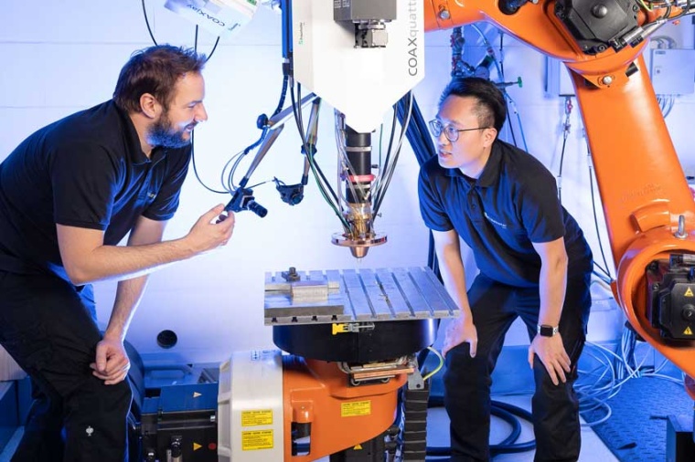
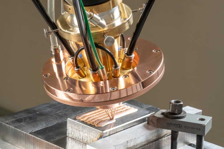
The Dresden-based institute and the company Laserline have now achieved and surpassed deposition rates with 20-kilowatt diode lasers which were previously only feasible using plasma-transferred arc processes (PTA). The partners have also made considerable progress compared to existing laser-based solutions: Depending on the specific material and the nozzle selected, HICLAD achieves deposition rates of 18 kilograms per hour in industrial use. For an Inconel 625 nickel alloy, for example, productivity can be roughly tripled compared to a solution using a conventional 9 kW laser. The exact values depend on the specific application scenario. Compared to competing solutions with high-power lasers, the Fraunhofer IWS process is considered more robust.
In contrast to powder-based laser cladding, wire-based processes were previously limited to a maximum of six kilowatts. COAXquattro now enables laser power of up to 20 kW to be used in the combination of wire and powder. This can play a decisive role in multimaterial development, for example of novel alloys. Different materials can be fed as required through each of four wire and powder channels. In addition, the comparatively short processing times shrink expenditures for staff, shielding gases and other operating costs. In general, the system is designed for particularly efficient material utilization as well as very robust and flexible process control with high quality.
Company
Laserline Gesellschaft für Entwicklung und Vertrieb von Diodenlasern mbHFraunhofer Straße 5
56218 Mülheim-Kärlich
Germany


most read

ZVEI Calls for Swift Protection of Critical Power Infrastructure
The association has issued a statement in response to the recent attempted attacks on substations in Brandenburg and North Rhine-Westphalia and warns of the consequences for Germany's energy security.
European machine vision expects slight recovery and growth in 2026
According to the VDMA Machine Vision department, sales are expected to increase by around 3%, following a decline of 2% in 2025.
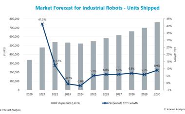
Forecast: Significant Growth in Industrial Robotics by 2030; Cobots Are Growing the Fastest
According to a recent analysis by Interact Analysis, global sales of industrial robots are expected to rise from about 550,000 units in 2025 to just over 760,000 units in 2030.
Solid-State Transformers for AI Data Centers
As part of a strategic partnership, Siemens and Reinhausen are developing a solid-state transformer for AI data centers with an 800-volt DC system.
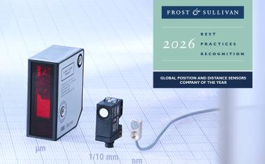
Baumer Honored as Company of the Year
Frost & Sullivan has named Baumer the 2026 Global Company of the Year in the Position and Distance Sensing category.