Mitutoyo Opens New Center of Excellence in Dresden
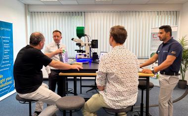
In a space of approximately 300 square meters, measurement systems with nanometer-level precision are available for practical demonstrations, testing in real-world applications, and personalized consulting.
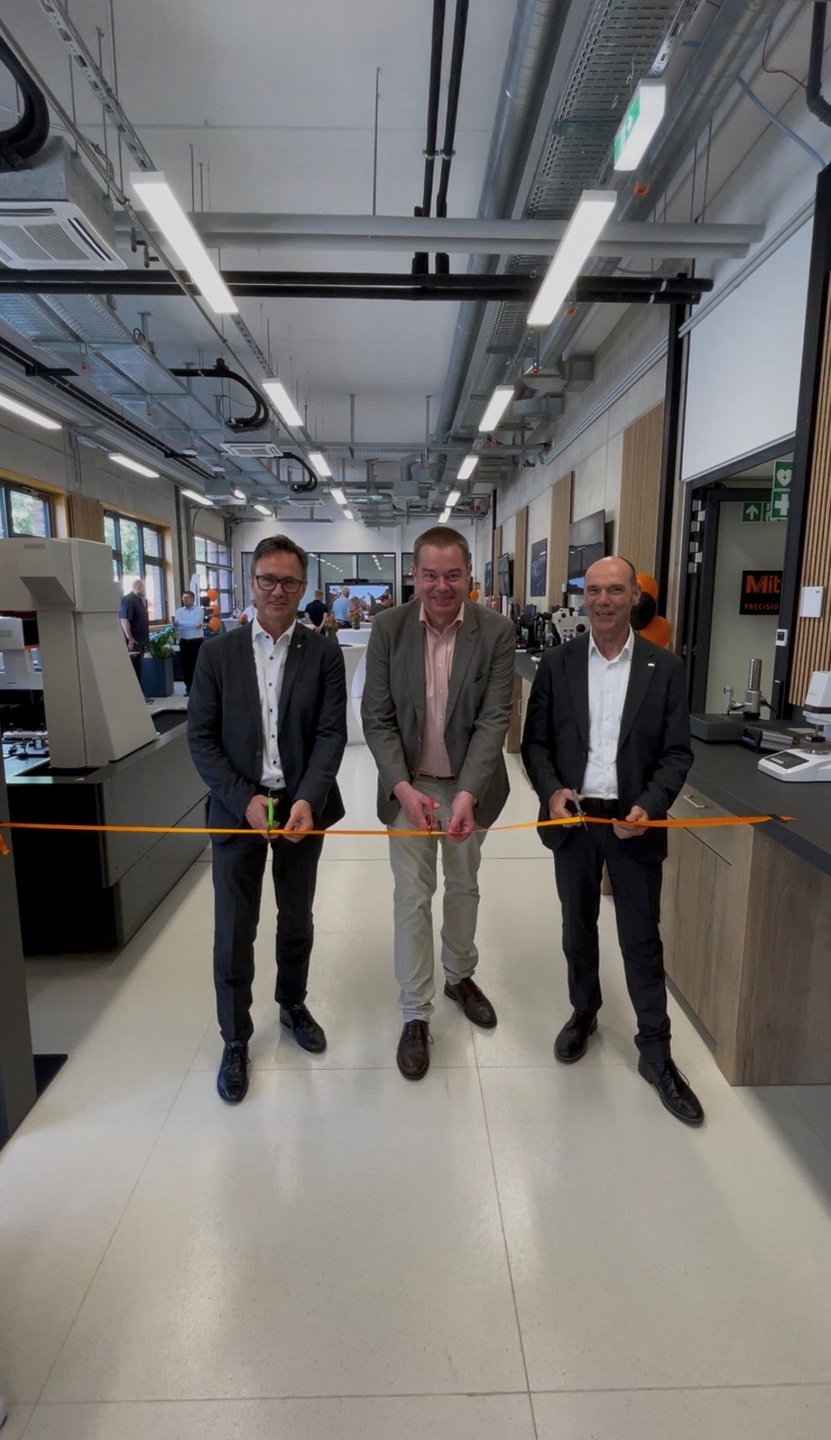
Mitutoyo has opened a semiconductor competence center in Dresden to provide more targeted support to customers in the Silicon Saxony region. Spanning approximately 300 square meters, the center features nanometer-precise measurement systems for practical demonstrations, testing in real-world applications, and personalized consulting. In addition, Mitutoyo offers training and certification programs tailored to the requirements of semiconductor manufacturing.
This local presence is intended to shorten communication channels, accelerate decision-making processes, and facilitate direct exchange between users and metrology experts. The choice of location reflects the dynamic development of the regional semiconductor ecosystem and the investments by major chip manufacturers, which require close cooperation along the value chain. With this center, Mitutoyo aims to help increase process reliability, shorten time-to-market, and strengthen its customers’ competitiveness.