Integrated light as a key to future computers
Brunswick and Jena cooperate on optoelectronic components in the federally-funded OptoGaN project.
While computer chips are getting smaller and faster every year, one challenge remains unsolved: combining electronics and photonics on a single chip. Although components such as microLEDs are available as individual chips and waveguides as tiny fiber optic cables, the materials required are too different for a harmonized chip. A new type of etching process could now be the decisive breakthrough for combining light sources and optical fibers. In the OptoGaN project, researchers from the TU Braunschweig and the Friedrich Schiller University Jena are therefore working on porous gallium nitride.
It will be particularly worthwhile for the strong German photonics industry to take a close look at Brunswick and Jena over the next few years. The joint idea of the participating research groups offers a wide range of potential applications. The project partners want to realise three of these ideas as demonstrators together with one start-up each. These will then benefit technologies such as waveguides, neuromorphic computers and the Quantum Valley Lower Saxony‘s ion trap quantum computer. At the same time, the newly founded Nitride Technology Center (NTC) at TU Braunschweig will support the further development of nitride technology at the highest level and bring it into application.
But what are the potential applications for this new technology? For example, quantum computers still need large laser systems to manipulate their ions. If more and more quantum bits are to be calculated together in the computer, this laser system must become significantly smaller – at best the size of a chip. However, the standard material silicon dioxide for waveguides on chips absorbs precisely the critical wavelengths of light. The porous gallium nitride could offer an alternative here and bring the customized light to the individual ion with minimal loss.
Complementary expertise in handling gallium nitride
The porous semiconductor is based on a new selective etching process. The researchers use it to create elongated, air-filled channels – pores – in the gallium nitride structures. This even makes three-dimensional waveguides with complex optical light guidance conceivable. As gallium nitride and the process are compatible with existing LED production methods, integrated electronic and photonic circuits will also be possible.
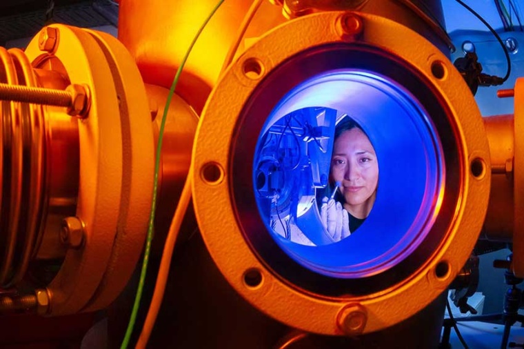
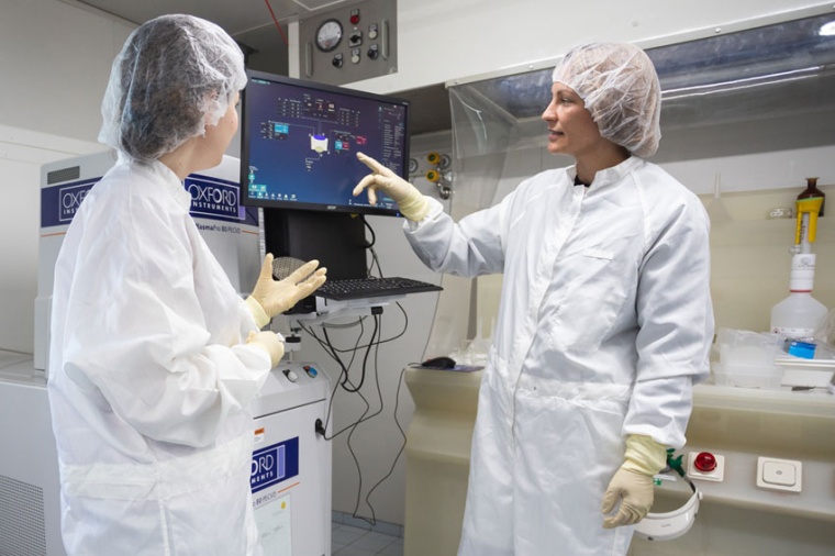
In order to realize the innovative semiconductor channels for light guidance, the researchers from Brunswick and Jena are bringing together complementary expertise and special equipment. This is because the etching process used here has both an electronic and a chemical component. Firstly, the Brunswick researchers produce the base material layer by layer. The semiconductor chip then travels to Jena for ion implantation. The researchers from Jena dope the chip and change its electronic properties in a targeted manner. Finally, the chip has to return to Brunswick, where the chemical etching process forms the final, porous structure.
The project
The project Highly integrated microphotonic modules in nitride technologies, OptoGaN for short, is being funded by the Federal Ministry of Education and Research with around 600,000 euros. The TU Braunschweig’s share of the funding amounts to 450,000 euros. The partners from TU Braunschweig and Friedrich Schiller University Jena started OptoGaN in 2023 for three years until October 2026.
Company
Friedrich Schiller University JenaMain University Building (Universitätshauptgebäude)
07743 Jena
Germany


most read

Edmund Optics Receives the “2026 Private Company Boards of the Year Award”
The awards recognize the supervisory boards of private companies that demonstrate exemplary corporate governance, strategic foresight, and sustainable value creation.
Logimat 2027 Focuses on the Interaction Between People and Technology
Under the theme “Mind meets machine – what's next?”, the trade show focuses on the interplay between human expertise and technological systems.
Igus Expands Its Bicycle Line with an Electric Model
The new e-bike is designed for urban use and features a 60 Nm rear-wheel motor, a carbon-fiber and plastic toothed belt, and a battery with a range of up to 120 kilometers.
New Jumo advertising tower with LED technology and a rotating logo in Fulda
The company has replaced the old tower at its Fulda site with a technically upgraded facility.
27th VDI Automation Congress: Laying the Groundwork for Industrial AI and Automation
The 27th VDI Automation Congress in Baden-Baden focused on digital data sovereignty in future industrial AI applications.