Easier production of photonic MEMS
New switch that uses existing fabrication method is a step toward integration in data networks.
One of the technical challenges the current data revolution faces is finding an efficient way to route the data. This task is usually performed by electronic switches, while the data itself is transferred using light confined in optical waveguides. For this reason, conversion from an optical to an electronic signal and back-conversion are required, which costs energy and limits the amount of transferable information. These drawbacks are avoidable with a full optical switch operation. One of the most promising approaches is based on microelectromechanical systems (MEMS), thanks to decisive advantages such as low optical loss and energy consumption, monolithic integration, and high scalability. Indeed, the largest photonic switch ever demonstrated uses this approach.
Until now, those MEMS photonic switches have been fabricated using nonstandard and complex processes in laboratory environments, which has made their commercialization difficult. But University of California Berkeley researchers initiated a collaboration that gathered engineers from different universities worldwide to demonstrate that the difficulties could be overcome. They created a photonic MEMS switch using a commercially available complementary metal-oxide-semiconductor (CMOS) fabrication process without modification. The use of this well-known microfabrication platform represents a huge step toward industrialization because it is compatible with most current technologies, cost-effective, and suited for high-volume production.
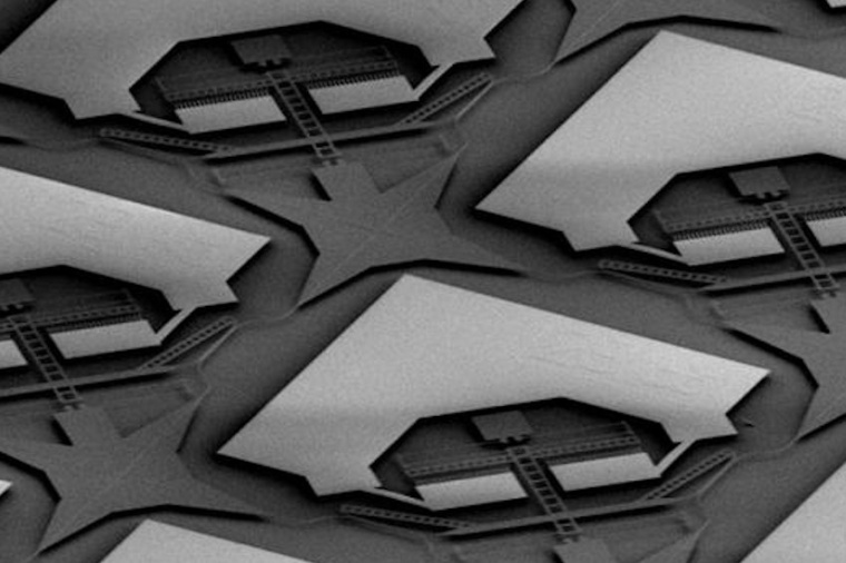
In their research, the photonic switch was fabricated on silicon-on-insulator (SOI) 200-mm wafers using regular photolithographic and dry-etching processes in a commercial foundry. The whole photonic integrated circuit is included in the silicon top layer, which has the advantage of limiting the number of fabrication steps: There are two different dry-etching processes, one lift-off to create metal interconnects, and the final release of the MEMS by oxide etching. The switch design includes 32 input ports and 32 output ports, representing a 32 x 32 matrix of the same replicated element. In each of the single elements, the light transfer from one channel to the other is produced by decreasing the distance between two waveguides to couple their modes, an operation achieved by an electrostatic comb drive also included in the silicon top layer.
“For the first time, large-scale and integrated MEMS photonic switches have been fabricated in a commercial foundry on 200-mm SOI wafers. In my opinion, this is a convincing demonstration that this technology is suited for commercialization and mass production. They could be incorporated in data communication systems in the near future,” said Jeremy Béguelin, one of the Berkeley researchers. The researchers evaluated the performance of the photonic switches by measuring several important parameters: the light power loss through the entire switch of 7.7 dB, the optical bandwidth of about 30 nm at the 1550 nm wavelength, and the speed of the switching operation of 50 μs. These values are already excellent in comparison with other photonic switch approaches, and ways to improve them have already been identified.
By using a CMOS-compatible fabrication process and SOI wafers, the research team created a robust and efficient photonic switch based on MEMS technology. Such work opens a promising path toward the commercialization and mass production of large and integrated photonic switches, a future key component of data communication networks. (Source: SPIE)
Link: Integrated Photonics Laboratory, University of California Berkeley, Berkeley, USA