

Photonic chip integrates sensing and computing
Technology eliminates optical-electronic conversions for ultrafast machine vision.
Researchers have demonstrated a new intelligent photonic sensing-computing chip that can process, transmit and reconstruct images of a scene within nanoseconds. This advance opens the door to extremely high-speed image processing that could benefit edge intelligence for machine vision applications such as autonomous driving, industrial inspection and robotic vision.
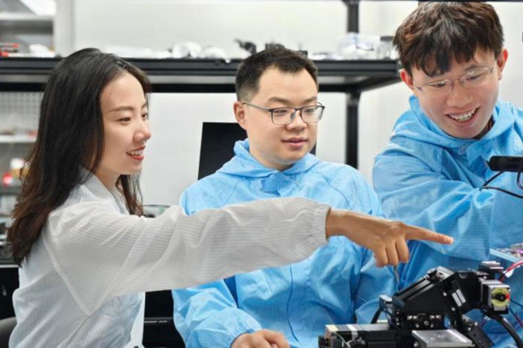
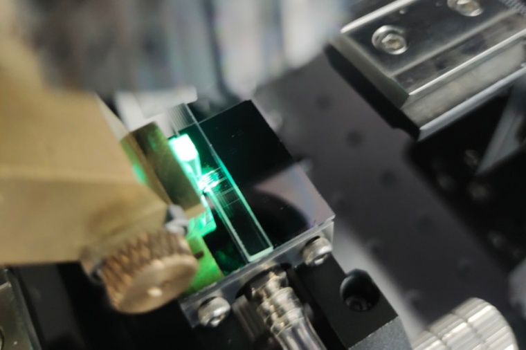
Edge computing, which performs intensive computing tasks like image processing and analysis on local devices, is evolving into edge intelligence by adding artificial intelligence (AI) driven analysis and decision-making. “Capturing, processing and analyzing images for edge-based tasks such as autonomous driving is currently limited to millisecond-level speeds due to the necessity of optical-to-electronic conversions,” said research team leader Lu Fang from Tsinghua University in China. “Our new chip can perform all these processes in just nanoseconds by keeping them all in the optical domain. This could be used to significantly enhance, or even replace, the traditional architecture of sensor acquisition followed by AI postprocessing.”
Now, the researchers describe the new chip, which they call an optical parallel computational array (OPCA) chip. They show that the OPCA has a processing bandwidth of up to one hundred billion pixels and a response time of just six nanoseconds, which is about six orders of magnitude faster than current methods. They also used the chip to create an optical neural network that integrates image perception, computation and reconstruction. “The chip and optical neural network could boost the efficiency of processing complex scenes in industrial inspection and help advance intelligent robot technology to a higher level of cognitive intelligence,” said Wei Wu. “We think it could also revolutionize edge intelligence.”
Machine vision – which uses cameras, image sensors, lighting and computer algorithms to capture, process and analyze images for specific tasks – traditionally involves converting optical information into digital electrical signals using sensors. These signals are then transmitted over optical fibers for long-distance data transmission and downstream tasks. However, the frequent conversion between optical and electrical signals along with limited advancements in electronic processors has become a major restriction on improving the speed and processing capacity of machine vision.
“The world is entering an AI era, but AI is very time- and energy-exhaustive,” said Fang. “Meanwhile, the growth of edge devices, such as smartphones, intelligent cars and laptops has resulted in explosive growth of image data to be processed, transmitted and displayed. We are working to advance machine vision by integrating sensing and computing in the optical domain, which is particularly important for edge computing and for enabling more sustainable AI applications.” The challenge in performing both image acquisition and analysis on the same chip in the optical domain is finding a way to convert the free-space spatial light used for imaging into an on-chip guided light wave. The researchers achieved this by designing a chip that consists of a sensing-computing array of dedicated designed ring resonators that convert a free-space optical intensity image – a 2D representation of a scene’s light intensity – into a coherent light signal that can then be guided on the chip. A micro-lens array enhances the process by focusing the scene onto the OPCA chip.
The chip’s architecture allowed the researchers to create an end-to-end multi-wavelength optical neural network to couple the on-chip modulated light into a large-bandwidth optical waveguide, where the modulated light is added together spectrally. The multispectral optical outputs can then be used for classification tasks or to create an all-optical reconstruction of the image. “Because each sensing-computing element of this chip is reconfigurable, they can each operate as a programmable neuron that generates light modulation output based on the input and weight,” said Fang. “The neural network connects all the sensing-computing neurons with a single waveguide, facilitating an all-optical full connection between the input information and the output.”
To demonstrate the capabilities of the OPCA chip, the researchers showed that it could be used to classify a handwritten image and to perform image convolution, a process that applies a filter to an image to extract features. The findings showed that the chip architecture can effectively complete information compression and scene reconstruction, indicating its potential for widespread applications.
The researchers are now working to improve the sensing-computing OPCA chip to further enhance computational performance while also being aligned more closely with real-world scenarios and optimized for edge computing applications. The researchers say that for practical use, the optical neural network's processing capacity would need to be increased to effectively handle increasingly complex and realistic intelligent tasks. The form factor of the OPCA chip and overall form factor also need to be minimized. “We hope that machine vision will be gradually improved to be faster and more energy-efficient by using light to perform both sensing and computing,” said Fang. “Even though today’s approach will not likely be completely replaced, we expect the sensing-computing method to find its niche in edge computing where it can drive a wide range of promising applications.” (Source: Optica)
Link: Dept. of Electronic Engineering, Tsinghua University, Beijing, China

most read
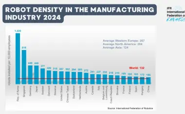
Global robot density: Western Europe leads ahead of North America and Asia
In the EU-27, the robot density is 231, which is above the global average of 132.

Siemens Consolidates Its Automation Business into a New Unit Called Automation
Rainer Brehm, who previously served as COO of the automation business and CTO of Digital Industries, was appointed president of the new unit.

ABB Machine Automation (B&R) Appoints Christian Strahberger as New Division President
He succeeds Florian Schneeberger, who died in a tragic accident in April.

Schaeffler bundles Defense and New Space activities under new CEO
Celia Pelaz takes over the position of CEO Defence & New Space at Schaeffler on October 1, 2026 and becomes Chairwoman of the Management Board of Stech Defence GmbH.

ZVEI Calls for Swift Protection of Critical Power Infrastructure
The association has issued a statement in response to the recent attempted attacks on substations in Brandenburg and North Rhine-Westphalia and warns of the consequences for Germany's energy security.