Paving the way for next-gen deep ultraviolet lasers
New laser improves the use of ultraviolet light for sterilizing medical tools, purifying water, sensing hazardous gases and enabling precision photolithography.
Cornell engineers have created a deep-ultraviolet laser using semiconductor materials that show great promise for improving the use of ultraviolet light for sterilizing medical tools, purifying water, sensing hazardous gases and enabling precision photolithography, among other applications. When it comes to ultraviolet light, two important qualities are frequency – certain frequencies are best for destroying viruses or sensing molecules – and linewidth, a measure of the laser’s precision. Scientists and engineers seek sources of higher quality, more efficient ultraviolet light emission, but it’s challenging to work with the semiconductor materials that can enable this.

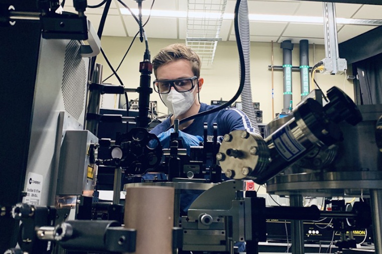
Now, Cornell scientists produced an aluminum gallium nitride-based device capable of emitting a deep-ultraviolet laser at sought-after wavelengths and modal linewidths. “It is known that this is a material that is suitable, but it was a materials synthesis problem,” said Len van Deurzen, a doctoral student in applied and engineering physics who led the research. “The challenge is making the materials pure enough that they're actually going to be useful and sustain the requirements of a laser.”
It was a challenge van Deurzen accepted during the COVID-19 pandemic when the market began to boom for ultraviolet LEDs and other tools capable of detecting and eliminating the SARS-CoV-2 virus. “I wanted a research project that could have impact,” van Deurzen said, “and the pandemic really amplified the need for improved ultraviolet devices.” Under the guidance of Debdeep Jena and Huili Grace Xing, both professors of materials science and engineering and of electrical and computer engineering, the team used molecular beam epitaxy, a crystal growth technique, to grow a high-quality crystal of aluminum nitride.
“We need multiple aluminum gallium nitride layers stacked on top of each other and one important parameter is the interface quality between those layers,” van Deurzen said. “We can grow very sharp interfaces without the impurities and dislocations that form with other growth techniques.” The second challenge was to create an optical cavity from the stacked layers that could be used to trap the emitted light and promote stimulated emission, which is necessary for the laser. The cavity was created in the form of a small, micron-scale resonator on an aluminum nitride chip that van Deurzen was able to develop with the help of the Cornell NanoScale Science and Technology Facility.
Once completed, the laser was able to achieve peak gain at a wavelength of 284 nanometers and modal linewidths on the order of 0.1 nanometers. The linewidth is an order of magnitude more precise than similar devices and demonstrates the growth method’s applicability towards improved ultraviolet light emitters. The Cornell deep-ultraviolet laser is optically pumped, meaning it produces certain requirements for lasing by inputting photons into the device. The next step in the research, according to Jena, is using the same materials platform to realize a laser that is driven by an electrical current from a battery – a more practical energy source for commercially available light-emitting devices.
“Deep-ultraviolet lasers arguably are the final frontier in semiconductor materials and devices with immense long-term payoffs,” said Jena, the David E. Burr Professor of Engineering and the Richard E. Lunquist Sesquicentennial Faculty Fellow. “Yet it is also the kind of problem that a young graduate student can get into and make an immediate impact.” (Source: Cornell U.)
Link: Dept. of Applied and Engineering Physics (D. Jena), Cornell University, Ithaca, USA


