Icecube Neutrino Observatory: Hamamatsu Photonics Boosts Sensitivity with New Photodetectors
The detector array is installed in one cubic kilometer of clear Antarctic ice and detects Cherenkov light produced by neutrino interactions
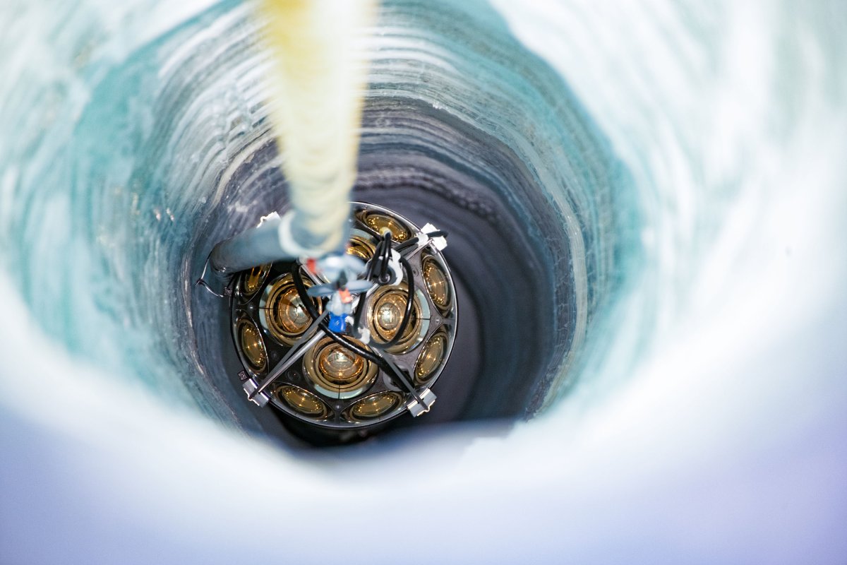
Hamamatsu Photonics is supporting the latest upgrade to the IceCube Neutrino Observatory at the Amundsen-Scott South Pole Station. The detector array is installed in one cubic kilometer of clear Antarctic ice and detects Cherenkov light produced during neutrino interactions. As part of the upgrade, five new sensor strings were installed to depths of approximately 2,400 meters and supplemented with more than 650 photodetectors and calibration units.
At the heart of the expansion are optical modules in which multiple PMTs are combined within a pressurized housing. This increases the effective photocathode area and improves the angular coverage of the light signals. In conjunction with advanced calibration procedures, this is intended to improve the precision of event reconstruction, reduce measurement uncertainties, and increase sensitivity to lower-energy neutrinos. This supports research into neutrino oscillations and astrophysical sources such as supernovae. Hamamatsu contributes photodetector technologies as well as expertise in qualification and integration for long-term operation under Antarctic conditions, laying the groundwork for future expansions such as IceCube-Gen2.