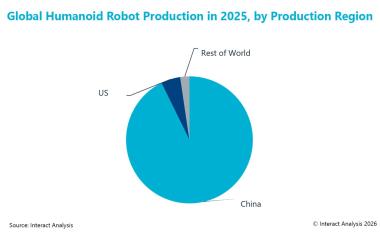
Hamamatsu expands production of microfocus X-ray sources
To meet the increasing demand, Hamamatsu Photonics has completed a new building for the production of microfocus X-ray sources (MFX) and other electron tube products.
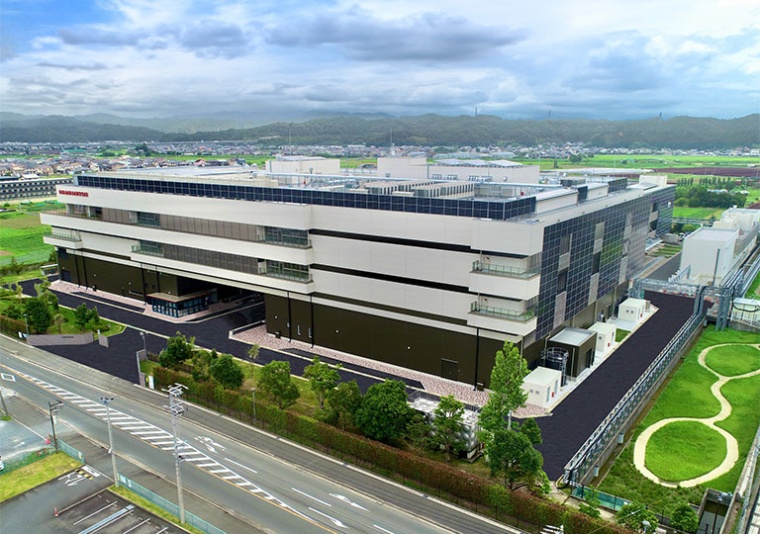
The recently completed Building No. 11 at Hamamatsu Photonics' Toyooka site will produce microfocus X-ray sources (MFX) and other electron tube products starting in August. It will be officially inaugurated on August 4, 2023.
Hamamatsu expects sales of these products to increase steadily. In particular, demand for microfocus X-ray (MFX) sources, which are used with imaging equipment in nondestructive testing of printed circuit boards for data servers and batteries for electric vehicles, is rising rapidly, so the company urgently needs more production capacity, Hamamatsu informs. With this expansion, the company expects to increase sales of its electron tube business to 100 billion yen (about 641 million euros) by the end of fiscal 2027.
The new building has an area of just over 24,000 square meters, which includes four floors for production and a canteen. It provides a total of 200 jobs. The construction cost around 64 million euros.