Applied Materials and CEA-Leti unveil joint lab
The collaboration focuses on developing differentiated materials engineering solutions for several specialty semiconductor applications.
Based at CEA-Leti, the joint lab aims to accelerate device innovations for Applied Material’s customers serving ICAPS markets – IoT, communications, automotive, power and sensors. Technology applications in those fields include photonics, image sensors, RF communications components, power devices and heterogeneous integration.
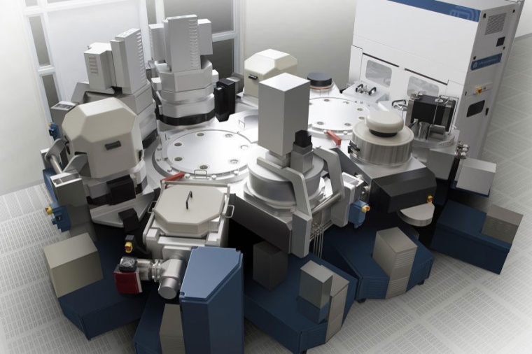
Demand for ICAPS applications and devices is being driven by industrial automation, the Internet of Things, electric vehicles, green energy and smart grid infrastructure, among other major high growth markets. Projects at the joint lab will focus on developing solutions for a variety of materials engineering challenges to enable the next wave of ICAPS device innovation. The joint lab features several of Applied Materials’ 200 and 300 mm wafer processing systems and leverages CEA-Leti’s world-class capabilities for evaluating performance of new materials and device validation. Improvements in power consumption, performance and area/cost, along with faster time to market (PPACt), will be key objectives of the joint team.
“For the past ten years, Applied Materials and CEA-Leti have collaborated through multiple, specific joint development programs, which have set the stage for establishing our new joint lab. In addition to developing differentiated technological solutions for Applied’s customers, the work performed at the joint lab will help overcome current technical hurdles in support of CEA-Leti’s internal R&D programs,” said Sébastian Dauvé, the institute’s CEO.