Thin metasurfaces instead of thick lenses
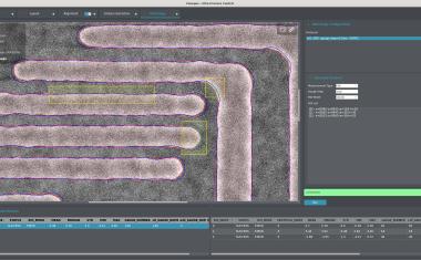
Producing metastructures on large surfaces with electron beam lithography.
Metasurfaces can help to make optical systems thinner in the future, while at the same time increasing their functionality. The problem: Until now, conventional manufacturing processes have often only been able to realize small metasurfaces, often smaller than one square millimeter. German researchers at Fraunhofer IOF have now succeeded for the first time in producing a metasurface with a diameter of almost 30 centimeters using electron beam lithography – a world record.
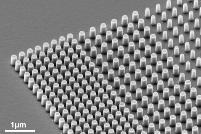
“After 500 years of lenses and mirrors, it is time to think ahead,” explains Falk Eilenberger, head of the Department of Micro- and Nanostructured Optics at the Fraunhofer Institute for Applied Optics and Precision Engineering IOF. Metasurfaces can be an alternative here. These are components that concentrate their complete optical function in a surface and achieve this function in the surface through nanostructures. Eilenberger explains the difference to the classic lens as follows: “In lenses, the function is defined by the macroscopic geometry. That's why the lens is thick and curved. Now we have a metasurface instead. It's thin and on scales smaller than the wavelength of light.”
Metasurfaces have been used in science and research for some time. However, the components here are often only a few square millimeters in size. This is sufficient for academic research, but not for many industrial applications, and certainly not to become a real alternative to the classic lens in the future. The researchers have therefore devoted themselves to the question of how innovative metasurfaces can be realized on a larger scale. As a result, they are now presenting a metasurface with a diameter of 30 centimeters for the first time. “We are not the inventors of metasurfaces,” Eilenberger holds. “But we are the only ones who can demonstrate it on such a large scale.”
“To produce our metasurface, we used a special writing strategy of electron beam lithography – character projection,” explains Uwe Zeitner, a researcher at Fraunhofer IOF. Character projection is a method in which a pattern is divided into smaller units. An electron beam is then used to create each of these small patterns in turn on a surface. This enables the fabrication of complex structures with high precision and efficiency. “Using character projection, very high-resolution structures can be exposed in parallel at comparatively high speeds. This is unusual for electron beam lithography,” Zeitner continues.
Together with his colleagues Michael Banasch and Marcus Trost, Zeitner has show that conventional lithographic techniques often reach their limits for fabricating larger structures. “Due to the small structure dimensions below the wavelength, high-resolution electron beam lithography is in principle very well suited for the fabrication of metastructures,” the researcher said. “However, this technology is relatively slow. So far essentially only elements with relatively small areas have been realized with it – primarily on the order of a few square millimeters. For larger areas, the exposure time very quickly reaches unrealistically large values.” By using character projection, the scientists were now able to address both the high resolution of electron beam lithography and the large element area without the exposure time exploding, according to Uwe Zeitner.
The new manufacturing technology can help build optical systems significantly thinner in the future. “This technology can revolutionize imaging optical systems,” says Falk Eilenberger, for example. “Because it will make it possible to reduce the size of systems while simultaneously increasing their optical functionality.” Uwe Zeitner adds concrete application examples: “Such large metasurfaces are particularly advantageous for compact optics in which large deflection angles are required in a small space. This is the case, for example, in virtual/augmented reality glasses. Advantageous designs can also be realized with such approaches for very small optics in smartphones.” Other potential applications include high-resolution spectroscopy or computer-generated holograms. (Source: Fh.-IOF)