Spectrometer on a chip
Tiny device is based on two-dimensional semiconductors and operated using artificial intelligence.
Scientists including an Oregon State University materials researcher have developed a better tool to measure light, contributing to optical spectrometry in a way that could improve everything from smartphone cameras to environmental monitoring. The study was led by Aalto University researchers and resulted in a powerful, ultrasmall spectrometer that fits on a microchip and is operated using artificial intelligence.
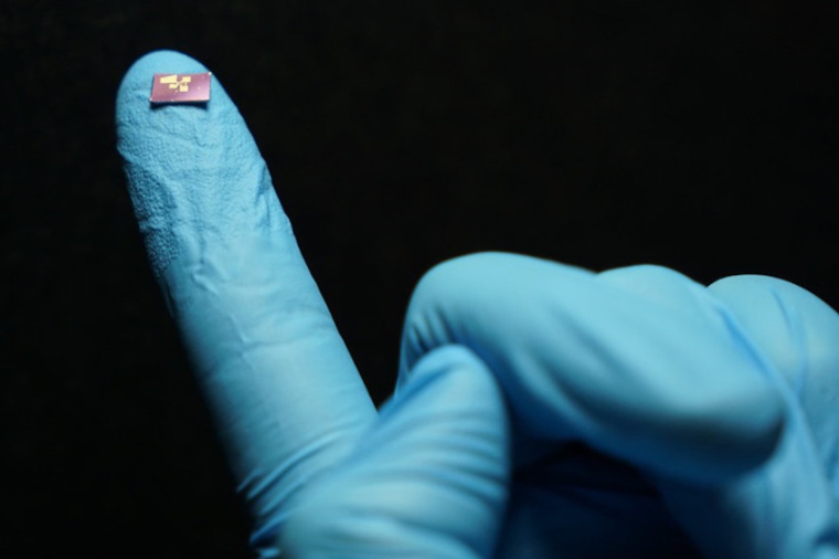
The research involved two-dimensional semiconductors and the upshot is a proof of concept for a spectrometer that could be readily incorporated into a variety of technologies – including quality inspection platforms, security sensors, biomedical analyzers and space telescopes. “We’ve demonstrated a way of building spectrometers that are far more miniature than what is typically used today,” said Ethan Minot at the OSU College of Science. “Spectrometers measure the strength of light at different wavelengths and are super useful in lots of industries and all fields of science for identifying samples and characterizing materials.”
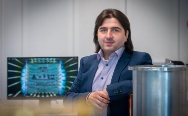
Traditional spectrometers require bulky optical and mechanical components, whereas the new device could fit on the end of a human hair, Minot said. The new research suggests those components can be replaced with novel semiconductor materials and AI, allowing spectrometers to be dramatically scaled down in size from the current smallest ones, which are about the size of a grape. “Our spectrometer does not require assembling separate optical and mechanical components or array designs to disperse and filter light,” said Hoon Hahn Yoon, who led the study with Aalto University colleague Zhipei Sun Yoon. “Moreover, it can achieve a high resolution comparable to benchtop systems but in a much smaller package.”
The device is 100 % electrically controllable regarding the colors of light it absorbs, which gives it massive potential for scalability and widespread usability, the researchers say. “Integrating it directly into portable devices such as smartphones and drones could advance our daily lives,” Yoon said. “Imagine that the next generation of our smartphone cameras could be hyperspectral cameras.” Those hyperspectral cameras could capture and analyze information not just from visible wavelengths but also allow for infrared imaging and analysis.
“It’s exciting that our spectrometer opens up possibilities for all sorts of new everyday gadgets, and instruments to do new science as well,” Minot said. In medicine, for example, spectrometers are already being tested for their ability to identify subtle changes in human tissue such as the difference between tumors and healthy tissue. For environmental monitoring, Minot added, spectrometers can detect exactly what kind of pollution is in the air, water or ground, and how much of it is there. “It would be nice to have low-cost, portable spectrometers doing this work for us,” he said. “And in the educational setting, the hands-on teaching of science concepts would be more effective with inexpensive, compact spectrometers.”
Applications abound as well for science-oriented hobbyists, Minot said. “If you’re into astronomy, you might be interested in measuring the spectrum of light that you collect with your telescope and having that information identify a star or planet,” he said. “If geology is your hobby, you could identify gemstones by measuring the spectrum of light they absorb.”
Minot thinks that as work with two-dimensional semiconductors progresses, “we’ll be rapidly discovering new ways to use their novel optical and electronic properties.” Research into 2D semiconductors has been going on in earnest for only a dozen years, starting with the study of graphene, carbon arranged in a honeycomb lattice with a thickness of one atom. “It’s really exciting,” Minot said. “I believe we’ll continue to have interesting breakthroughs by studying two-dimensional semiconductors.” (Source: OSU)
Link: QTF Centre of Excellence, Dept. of Applied Physics, Aalto University, Aalto, Finland • Nanoelectronics and Optoelectronics, Dept. of Physics, Oregon State University, Corvallis, USA