Bending light to enhance wavelength conversion
Plasmon-coupled surface states could improve imaging and sensing systems.
Electrical engineers from the University of California, Los Angeles, UCLA Samueli School of Engineering, have developed a more efficient way of converting light from one wavelength to another, opening the door for improvements in the performance of imaging, sensing and communication systems.
Finding an efficient way to convert wavelengths of light is crucial to the improvement of many imaging and sensing technologies. For example, converting incoming light into terahertz wavelengths enables imaging and sensing in optically opaque environments. However, previous conversion frameworks were inefficient and required bulky and complex optical setups. The team has devised a solution to enhance wavelength-conversion efficiency by exploring a generally undesirable but natural phenomenon of semiconductor surface states. Surface states occur when surface atoms have an insufficient number of other atoms to bind to, causing a breakdown in atomic structure. These incomplete dangling bonds cause roadblocks for electric charges flowing through semiconductor devices and affect their performance.
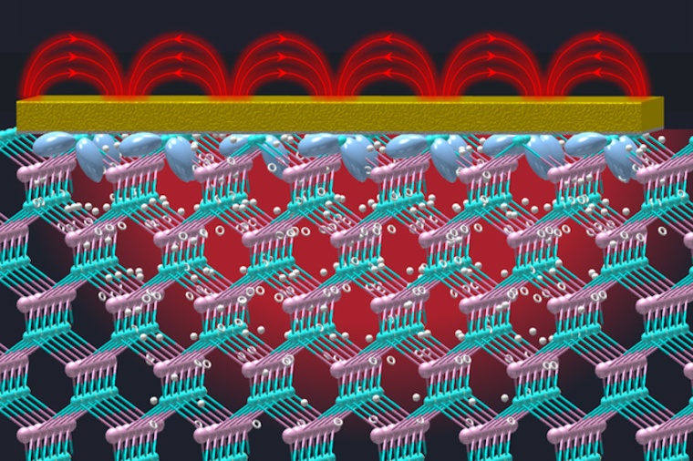
“There have been many efforts to suppress the effect of surface states in semiconductor devices without realizing they have unique electrochemical properties that could enable unprecedented device functionalities,” said Mona Jarrahi, who leads the UCLA Terahertz Electronics Laboratory. In fact, since these incomplete bonds create a shallow but giant built-in electric field across the semiconductor surface, the researchers decided to take advantage of surface states for improved wavelength conversion.
Incoming light can hit the electrons in the semiconductor lattice and move them to a higher energy state, at which point they are free to jump around within the lattice. The electric field created across the surface of the semiconductor further accelerates these photo-excited, high-energy electrons, which then unload the extra energy they gained by radiating it at different optical wavelengths, thus converting the wavelengths. However, this energy exchange can only happen at the surface of a semiconductor and needs to be more efficient. In order to solve this problem, the team incorporated a nanoantenna array that bends incoming light so it is tightly confined around the shallow surface of the semiconductor.
“Through this new framework, wavelength conversion happens easily and without any extra added source of energy as the incoming light crosses the field,” said Deniz Turan, a member of Jarrahi’s research laboratory. The researchers successfully and efficiently converted a 1,550-nanometer wavelength light beam into the terahertz part of the spectrum, ranging from wavelengths of 100 micrometers up to 1 millimeter. The team demonstrated the wavelength-conversion efficiency by incorporating the new technology into an endoscopy probe that could be used for detailed in-vivo imaging and spectroscopy using terahertz waves.
Without this breakthrough in wavelength conversion, it would have required 100 times the optical power level to achieve the same terahertz waves, which the thin optical fibers used in the endoscopy probe cannot support. The advance can apply to optical wavelength conversion in other parts of the electromagnetic spectrum, ranging from microwave to far-infrared wavelengths. (Source: UCLA)