Laser-based welding in lightweight construction
Projects Twin-Weld and MULTISPOT overcome the limitations of fixed bifocal optics and develop a welding head with a matrix of 3 × 3 laser diodes that can be individually controlled.
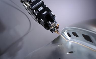
LMB Automation was engaged in two collaborations with research institutions and industry partners to improve laser welding under certain conditions, to overcome the limitations of fixed bifocal optics, and to implement the process on automotive parts.
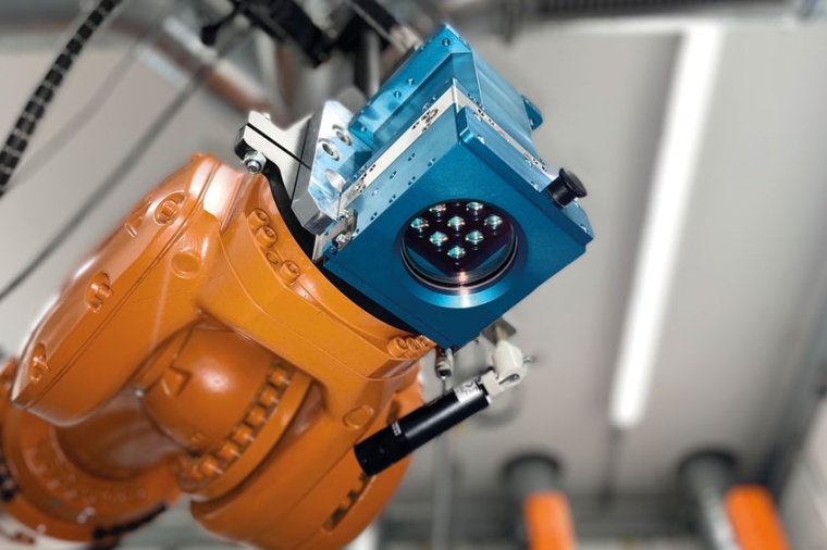
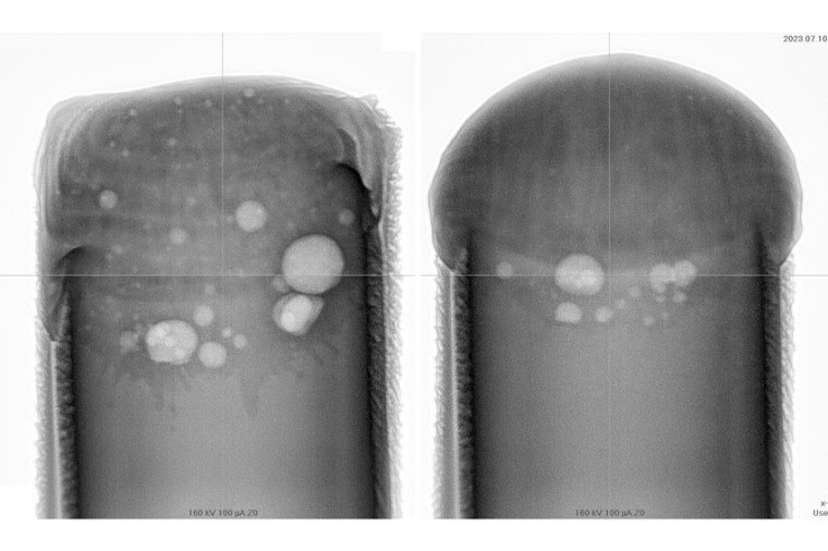
The laser beam tool has become an integral part of modern production, and the requirement for improved efficiency and new potential applications is continuously growing. With new fields of application, component geometries and materials, the conventional optics with limited movement and limited beam shaping options are often no longer able to guarantee a flawless welding result. Such applications include, for example, the joining of thermoplastics and metal as structural components in vehicle construction, and the welding of hairpins in electric motors. For this reason, the LMB laser specialists have developed two new concepts with partners that can be used to positively influence the melt pool through more flexible control and more precise power distribution. With the twin-weld process, better mixing in the melt pool is achieved so that gaps can be bridged more quickly. Multispot allows the intensity distribution within a laser focus to be varied locally and temporally. The performance can then be precisely adapted to the weld geometry and material properties.
Read the interactive issue in the Adobe Cloud, or download the single-article PDF – Laser-based welding in lightweight construction, PhotonicsViews 22 (D1), April 2025, pp. 35–39


most read

It Does Not Always Have to Be a Humanoid Robot
Mythomorphic design adds a distinct perspective to social robotics. Inspired by myths and fantasy rather than humans or animals, the article classifies examples and examines related opportunities and risks.

Protective Windows: Finding a Germanium Alternative for LWIR Imaging
In this interview, Mike Giznik, President of Midopt, explains why Silwir is a good choice for applications such as industrial inspection, defense, and autonomous systems.
The Rise of Photonic and Neuromorphic Computing: A New Era for AI Hardware
Computer Architectures for future data processing

Chatbots for Dead, Endangered, and Extinct Languages
Possibilities and Limitations of Generative AI for Continuing Education.
Automatic Defect Detection in Laser Welding and Brazing with AI
Process Monitoring in Automotive Production.