Zeiss Microscopy opens Semiconductor Applications Lab
State-of-the-art innovation laboratory in Dresden, Germany, pushes the limits of advanced semiconductor applications.
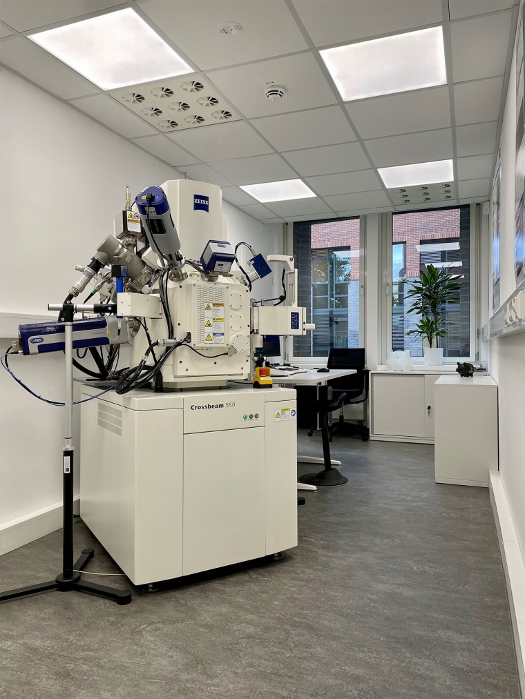
Zeiss has recently opened its Microscopy semiconductor applications lab in Dresden, a state-of-the-art facility dedicated to addressing physical analysis challenges and pushing the limits of nanoscale analysis with the Crossbeam focused ion beam-scanning electron microscope (FIB-SEM).
The new facility is strategically located in Dresden, the heart of semiconductor innovation within Europe, allowing for close collaboration with semiconductor industry customers and partners on physical failure analysis, materials development and process yield improvement for advanced logic and memory, power semiconductors, MEMS, advanced packaging, and more. The company will address increased automation of microscopy workflows and advanced techniques to help the semiconductor industry accelerate root cause analysis and pathfinding for the most challenging issues in microelectronics.
This laboratory in Dresden is the third major investment of Zeiss into semiconductor microscopy applications and strengthens the company’s global support capabilities. The Dresden team collaborates closely with its counterparts in Taiwan and Korea to share knowledge and best practices to best address customer needs across these three global hotspots of semiconductor excellence. Importantly, the advanced applications developed by these three teams will steer the innovation roadmap to meet the greatest challenges facing lab professionals in the semiconductor industry.
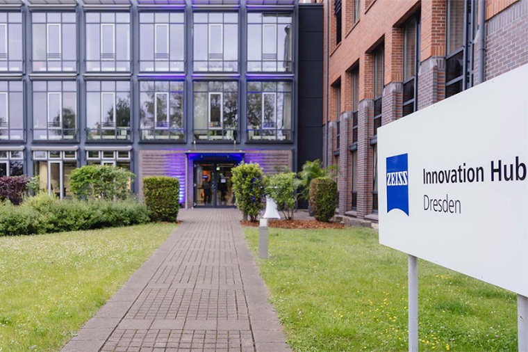
The semiconductor microscopy applications lab is located within the Innovation Hub Dresden that opened last May. The site complements Zeiss’ Innovation Center in Hsinchu Science Park, Taiwan, which opened in June 2024 and features a comprehensive portfolio to meet the productivity needs of semiconductor research and development, production and failure analysis. The third Innovation Center is in Dongtan, Korea, where the company develops applications across a complete portfolio of optical and electronic equipment, X-ray microscopy and high-resolution CT, and 3D metrology instruments.
Further reading: Zeiss expands its Innovation Hub in Dresden, wileyindustrynews.com, 17 May 2024 • Werner von Siemens Ring goes to Zeiss and Trumpf, wileyindustrynews.com, 18 September 2024
Company
Carl Zeiss AGCarl-Zeiss-Str. 22
73447 Oberkochen
Germany


most read

5 robotics trends for 2026
The International Federation of Robotics reports on the five most important trends for the robotics industry in 2026.
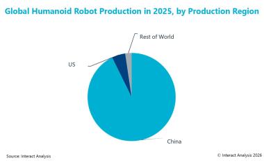
The market for humanoid robots is growing rapidly
Global production of humanoid robots rose to over 20,000 units in 2025, a tenfold increase compared to 2024.
Siemens takes over Canopus AI
This expansion of the Siemens EDA software portfolio is designed to help chip manufacturers improve precision and efficiency in wafer and mask inspection processes.
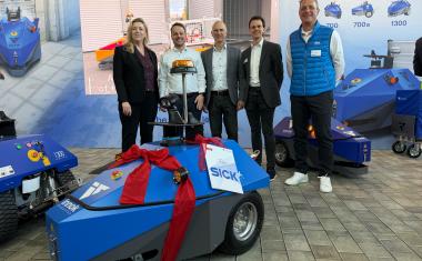
Sick and Innok Robotics intensify partnership in the field of outdoor robotics
Both companies are now working on technological developments.
Sick increases sales in 2025
In the 2025 financial year, the company increased its turnover to 1.85 billion euros, an increase of 6.5% compared to the previous year.