Evolution of light within photonic chips
New approach is paving the way to new applications in communication, imaging and quantum computing.
The field of photonic integrated circuits focuses on the miniaturization of photonic elements and their integration in photonic chips. Silicon-based photonics is a developing field that is relevant for data centers, artificial intelligence, quantum computing, and more. It enables an enormous improvement in the chips’ performance, and in their cost-benefit ratio as it is based on the very same prevalent raw material from chips in the world of electronics. However, despite benefiting from the well-developed lithography production process, which enables precise production of the desired devices, the instruments don’t yet enable accurate mapping of the chip’s optic characteristics. This includes its internal light motion – a crucial capacity given the difficulty to model the effect of fabrication flaws and inaccuracies – due to the devices’ tiny dimensions.
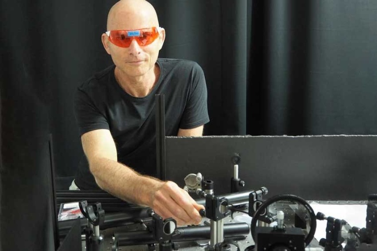
Now, researchers from Technion’s Andrew and Erna Viterbi Faculty of Electrical and Computer Engineering tackle this challenge, showing advanced light imaging in photonic circuits on chips. The research was led by Bartal, head of the Laboratory for Advanced Photonic Research, and doctoral student Matan Iluz, in collaboration with Rosenthal’s research group. Graduate students Kobi Cohen, Jacob Kheireddine, Yoav Hazan and Shai Tsesses also took part in the research.
The researchers harnessed the optical characteristics of silicon to map the light’s propagation without requiring an invasive action of any sort, which perturbs or alters the chip. This process includes mapping the light waves’ electric field and defining the elements that affect the light’s movement – waveguides and beam splitters.
The process provides real-time images and video recordings of the light inside the photonic chip, without having to damage the chip and without losing any data. This new process is expected to improve the design, production, and optimization processes of photonic chips in a variety of fields, including telecommunications, high-performance computing, machine learning, measuring distances, medical imaging, sensing, and quantum computing. (Source: Technion)
Link: Advanced Photonics Research Lab (APRL), Technion – Israel Institute of Technology, Haifa, Israel


