European project develops tap-proof communication solution
Project Silicon Photonics for Trusted Electronic Systems “Silhouette“ is launched.
As digitization continues, connected devices are making their way into more and more areas of everyday life. However, these are often vulnerable to cyberattacks; in the past, many end consumers, such as users of online services, were affected in addition to industry and businesses. A German consortium of industry, university and research institutes aims to make these systems more secure in the future thanks to light-based data transmission and computation. Over the next three years, the Silicon Photonics for Trusted Electronic Systems “Silhouette” project will develop universally applicable solutions. The German Federal Ministry for Education and Research BMBF is funding the project with around twelve million euros.
With the Internet of Things (IoT), i.e. the networking of numerous intelligent physical and virtual objects, numerous applications are already generating added value for industry, logistics and business. By 2025, an increase from 30 to 75 billion IoT devices is forecast. Accordingly, global efforts are underway to improve the security of these assets to protect sensitive data from misuse by third parties. Strong, hardware-supported cryptographic algorithms are one of the methods being used to achieve this. However, with increasing communication speeds, the negative cost and energy budget grows.
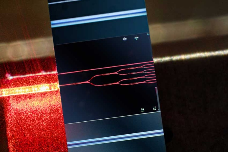
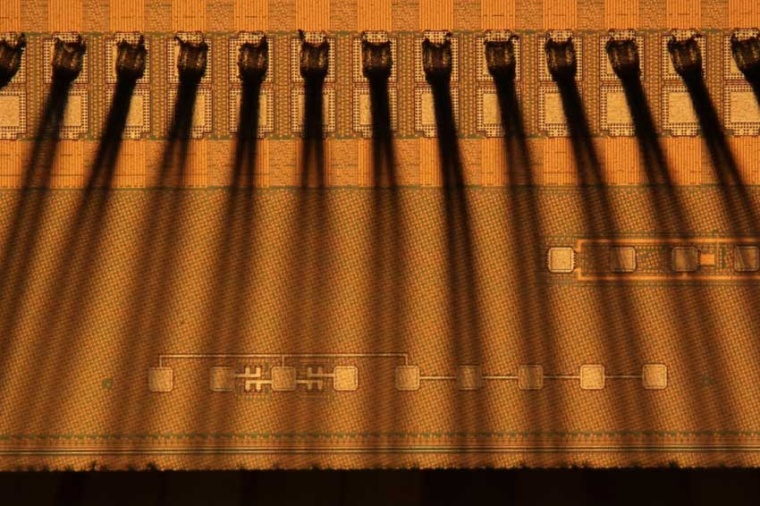
“By expanding silicon-based technologies to include photonic, i.e. light-based, special components, we can address this issue,” explains Marcus Pietzsch, a scientist at the Fraunhofer Institute for Photonic Microsystems IPMS in Dresden and coordinator of the Silhouette project. The project aims to create a universal platform solution for developing such hybrid systems. The key point is to convert safety-critical electrical signals into optical signals, further process or validate them and finally convert them back. “Photonic transmission channels alone offer the advantage of being both virtually impossible to manipulate and tap-proof,” Pietzsch continues.
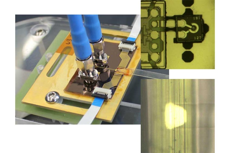
The hybrid approach of the consortium allows the use of existing safety-critical components from third-party suppliers, so that the current range of applications can ideally be maintained. The project covers the entire value chain: from the design of the electrical and optical components, through manufacturing, assembly and interconnection technology, to testing and inspection. Particular attention is being paid to ensure short time-to-market. “At present, it is still difficult to produce hybrid electro-optical circuits cost-effectively and in large quantities,” says Pietzsch. Therefore, the project partners will pool their expertise to develop prototypes which already contain features of secure products suitable for mass production.
European platform solution addresses trustworthiness and technological sovereignty
The desired electro-optical (E/O) platform solution is “made in Europe” in order to be able to guarantee technological sovereignty and trustworthiness also in the design and manufacturing process. In contrast to microelectronics, Germany can demonstrate a development lead in photonics across the board. “In order to maintain this lead and, in perspective, achieve sovereignty in manufacturing, photonic components must be more accessible. The prerequisite for this is the simplest possible universal interface to existing digital components, which will continue to be indispensable,” says Pietzsch.
The largest market segment for photonic components currently is the telecommunications sector. The photonic security technologies developed in project “Silhouette” are therefore geared to the specific security requirements of this market segment. “Subject areas beyond this, such as AI, simulation and complex mathematical optimization problems, are either still in the development or prototype stage or are being manufactured as small series with low volumes,” explains Pietzsch. “The consortium sees great potential here to make these technologies accessible to a broad user group and at the same time to open up completely new fields of application.”
Company
Fraunhofer Institut für Photonische Mikrosysteme IPMSMaria-Reiche-Str. 2
01109 Dresden
Germany


most read
TUM develops first European AI chip in 7 nm technology
The neuromorphic chip based on TSMC standards was developed under the leadership of Prof. Hussam Amrouch.

Engineering labor market under pressure: shortage of skilled workers despite the crisis
Unemployment in IT and engineering professions rose by 17.6 percent, while the total number of vacancies fell by 23 percent to 99,470.

Portwell acquires majority stake in Wincomm
The aim is to strengthen edge AI solutions
Sick increases sales in 2025
In the 2025 financial year, the company increased its turnover to 1.85 billion euros, an increase of 6.5% compared to the previous year.

TPL Vision joins EMVA
The company is looking forward to working together and sharing knowledge within the industry