Automatic Defect Review
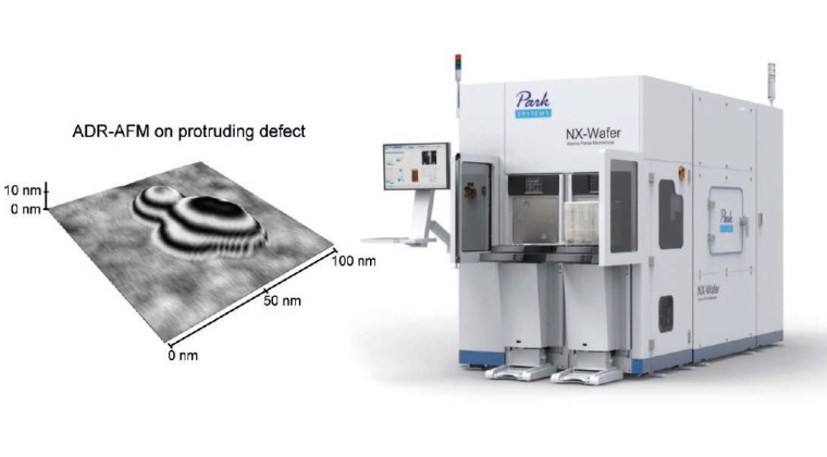
Advances in lithographic processing allow for the production of ever smaller semiconductor devices. With decreasing device sizes, nanometer-sized defects on the wafer substrates can already limit the performance of the devices.
The detection and classification of these defects requires characterization methods with a resolution in the nanometer-range. Due to the diffraction limit of visible light, the conventional automatic optical inspection (AOI) cannot achieve a sufficient resolution in that range, which impairs quantitative imaging and consequent classification of defects. The automatic defect review (ADR) with atomic force microscopy (AFM), on the other hand, visualizes defects in three dimensions with the nanometer-resolution customary for AFM. Thereby, ADR-AFM reduces uncertainties in the defect classification and qualifies as ideal technique for defect review in the semiconductor industry.