Vieworks relocated its headquarters and renew its corporate identity
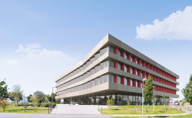
In September Vieworks relocated its headquarters to Anyang-city, Gyeonggi-province, Republic of Korea. The relocation to its newly constructed building in the new location is for the investment in manufacturing facilities and improvement of work conditions. Furthermore, the relocation to one of the most accessible cities in Korea is expected to give positive impacts on the company's aspiration for growth to a global level as a leading imaging solution company. The new headquarters exudes the corporation's pursuit of high business growth and confidence in becoming the leader of vision technology.
In the new facilities, Vieworks expects to improve production capacity and secure more human resources for all functions, especially in R&D center. In addition, sufficient space will induce advanced quality assurance systems to minimize field quality issues and the company expects to develop much more new products of highest quality.
Along with the relocation of headquarters, Vieworks has changed its corporate identity and slogan, "Imaging Expert" to express the company's pursuit to be an expert in machine vision industry. All the employees of Vieworks are set to make their best efforts in creating values by offering a better view, a better vision and a better imaging solution.