New way to fabricate optical qubits in silicon
A programmable approach to produce qubits for large-scale manufacturing.
Quantum computers have the potential to solve complex problems in human health, drug discovery, and artificial intelligence millions of times faster than some of the world’s fastest supercomputers. A network of quantum computers could advance these discoveries even faster. But before that can happen, the computer industry will need a reliable way to string together billions of qubits with atomic precision. Connecting qubits, however, has been challenging for the research community. Some methods form qubits by placing an entire silicon wafer in a rapid annealing oven at very high temperatures. With these methods, qubits randomly form from defects in silicon’s crystal lattice. And without knowing exactly where qubits are located in a material, a quantum computer of connected qubits will be difficult to realize.
Now, getting qubits to connect may soon be possible. A research team led by Lawrence Berkeley National Laboratory (Berkeley Lab) says that they are the first to use a femtosecond laser to create and annihilate qubits on demand, and with precision, by doping silicon with hydrogen. The advance could enable quantum computers that use programmable optical qubits or spin-photon qubits to connect quantum nodes across a remote network. It could also advance a quantum internet that is not only more secure but could also transmit more data than current optical-fiber information technologies.
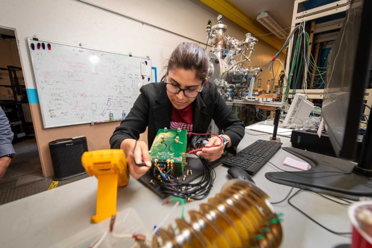
“To make a scalable quantum architecture or network, we need qubits that can reliably form on-demand, at desired locations, so that we know where the qubit is located in a material. And that's why our approach is critical,” said Kaushalya Jhuria, a postdoctoral scholar in Berkeley Lab’s Accelerator Technology & Applied Physics (ATAP) Division. “Because once we know where a specific qubit is sitting, we can determine how to connect this qubit with other components in the system and make a quantum network,” she says.
“This could carve out a potential new pathway for industry to overcome challenges in qubit fabrication and quality control,” said principal investigator Thomas Schenkel, head of the Fusion Science & Ion Beam Technology Program in Berkeley Lab’s ATAP Division. His group will host the first cohort of students from the University of Hawaii in June as part of a DOE Fusion Energy Sciences-funded RENEW project on workforce development where students will be immersed in color center/qubit science and technology.
The new method uses a gas environment to form programmable defects – color centers – in silicon. These color centers are candidates for special telecommunications qubits or spin photon qubits. The method also uses an ultrafast femtosecond laser to anneal silicon with pinpoint precision where those qubits should precisely form. A femtosecond laser delivers very short pulses of energy within a quadrillionth of a second to a focused target the size of a speck of dust. Spin photon qubits emit photons that can carry information encoded in electron spin across long distances – ideal properties to support a secure quantum network. Qubits are the smallest components of a quantum information system that encodes data in three different states: 1, 0, or a superposition that is everything between 1 and 0.
With help from Boubacar Kanté, a faculty scientist in Berkeley Lab’s Materials Sciences Division, the team used a near-infrared detector to characterize the resulting color centers by probing their photoluminescence signals. What they uncovered surprised them: a quantum emitter called the Ci center. Owing to its simple structure, stability at room temperature, and promising spin properties, the Ci center is an interesting spin photon qubit candidate that emits photons in the telecom band. “We knew from the literature that Ci can be formed in silicon, but we didn’t expect to actually make this new spin photon qubit candidate with our approach,” Jhuria said.
The researchers learned that processing silicon with a low femtosecond laser intensity in the presence of hydrogen helped to create the Ci color centers. Further experiments showed that increasing the laser intensity can increase the mobility of hydrogen, which passivates undesirable color centers without damaging the silicon lattice, Schenkel explained. A theoretical analysis performed by Liang Tan, staff scientist in Berkeley Lab’s Molecular Foundry, shows that the brightness of the Ci color center is boosted by several orders of magnitude in the presence of hydrogen, confirming their observations from laboratory experiments. “The femtosecond laser pulses can kick out hydrogen atoms or bring them back, allowing the programmable formation of desired optical qubits in precise locations,” Jhuria said.
The team plans to use the technique to integrate optical qubits in quantum devices such as reflective cavities and waveguides, and to discover new spin photon qubit candidates with properties optimized for selected applications. “Now that we can reliably make color centers, we want to get different qubits to talk to each other – which is an embodiment of quantum entanglement – and see which ones perform the best. This is just the beginning,” said Jhuria.
“The ability to form qubits at programmable locations in a material like silicon that is available at scale is an exciting step towards practical quantum networking and computing,” said Cameron Geddes, Director of the ATAP Division. (Source: DOE / LBL)