More sensitive X-ray imaging
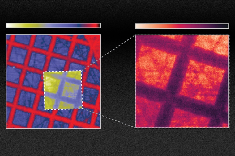
Researchers at MIT have shown how one could improve the efficiency of scintillators by changing the material’s surface to create certain nanoscale configurations.
Scintillators emit light when bombarded with high-energy particles or X-rays. In medical or dental X-ray systems, they convert incoming X-ray radiation into visible light that can then be captured using film or photosensors. They’re also used for night-vision systems and for research, such as in particle detectors or electron microscopes. Researchers at MIT have now shown how one could improve the efficiency of scintillators by at least tenfold, and perhaps even a hundredfold, by changing the material’s surface to create certain nanoscale configurations, such as arrays of wave-like ridges. While past attempts to develop more efficient scintillators have focused on finding new materials, the new approach could in principle work with any of the existing materials.

Though it will require more time and effort to integrate their scintillators into existing X-ray machines, the team believes that this method might lead to improvements in medical diagnostic X-rays or CT scans, to reduce dose exposure and improve image quality. In other applications, such as X-ray inspection of manufactured parts for quality control, the new scintillators could enable inspections with higher accuracy or at faster speeds.
The new approach applies advances in nanotechnology to existing materials. By creating patterns in scintillator materials at a length scale comparable to the wavelengths of the light being emitted, the team found that it was possible to dramatically change the material’s optical properties. “To make those nanophotonic scintillators”, Roques-Carmes says, “you can directly make patterns inside the scintillators, or you can glue on another material that would have holes on the nanoscale. The specifics depend on the exact structure and material.” For this research, the team took a scintillator and made holes spaced apart by roughly one optical wavelength, or about 500 nanometers.
“The key to what we’re doing is a general theory and framework we have developed,” Rivera says. This allows the researchers to calculate the scintillation levels that would be produced by any arbitrary configuration of nanophotonic structures. The scintillation process itself involves a series of steps, making it complicated to unravel. The framework the team developed involves integrating three different types of physics, Roques-Carmes says. Using this system they have found a good match between their predictions and the results of their subsequent experiments.
The experiments showed a tenfold improvement in emission from the treated scintillator. “So, this is something that might translate into applications for medical imaging, which are optical photon-starved, meaning the conversion of X-rays to optical light limits the image quality. [In medical imaging,] you do not want to irradiate your patients with too much of the X-rays, especially for routine screening, and especially for young patients as well,” Roques-Carmes says. “We believe that this will open a new field of research in nanophotonics,” he adds. “You can use a lot of the existing work and research that has been done in the field of nanophotonics to improve significantly on existing materials that scintillate.”
Soljacic says that while their experiments proved a tenfold improvement in emission could be achieved, by further fine-tuning the design of the nanoscale patterning, “we also show that you can get up to 100 times [improvement], and we believe we also have a path toward making it even better,” he says. Soljacic points out that in other areas of nanophotonics, a field that deals with how light interacts with materials that are structured at the nanometer scale, the development of computational simulations has enabled rapid, substantial improvements, for example in the development of solar cells and LEDs. The new models this team developed for scintillating materials could facilitate similar leaps in this technology, he says.
Nanophotonics techniques “give you the ultimate power of tailoring and enhancing the behavior of light,” Soljacic says. “But until now, this promise, this ability to do this with scintillation was unreachable because modeling the scintillation was very challenging. Now, this work for the first time opens up this field of scintillation, fully opens it, for the application of nanophotonics techniques.” More generally, the team believes that the combination of nanophotonic and scintillators might ultimately enable higher resolution, reduced X-ray dose, and energy-resolved X-ray imaging.
Yablonovitch adds that while the concept still needs to be proven in a practical device, he says that, “After years of research on photonic crystals in optical communication and other fields, it's long overdue that photonic crystals should be applied to scintillators, which are of great practical importance yet have been overlooked” until this work. (Source: MIT)
Link: Research Laboratory of Electronics, Massachusetts Institute of Technology, Cambridge, USA


