Measuring defects to better understand quantum systems
Researchers develop a new method to measure defects in diamond quantum systems, crucial for improving sensor stability and reliability.
Quantum defects have the potential to act as ultra-sensitive sensors that could offer new kinds of navigation or biological sensor technology. One type of these defect systems, nitrogen vacancy (NV) centers in diamonds, can measure nanoscale magnetic fields. But while scientists can control the quantum spin of these centers – single defects in the diamond, where nitrogen has replaced the carbon – they still do not have a full understanding of how to best isolate that spin from the spins of other defects in the material, which can destroy its quantum state memory, or coherence.
Only by studying exactly how this material works at the atomic level can scientists and engineers realize these sensors’ potential. In new research at the University of Chicago Pritzker School of Molecular Engineering (PME), researchers in the lab of David Awschalom have devised a new way to harness the defect spin to measure the behavior of other single electron defects in the diamond. This new understanding will be used to create even better quantum sensors that can maintain long coherence times. “We have devised a way to see certain behavior of single quantum spin states that have otherwise proven elusive to standard measurements,” Awschalom said. “This will impact both how we engineer quantum systems and how we think about charge in many materials.”
Led by Jonathan Marcks, the research team synthesizes these NV centers in facilities at Argonne National Laboratory. They grow diamond layer-by-layer through chemical vapor deposition, and can introduce only a few nanometers of nitrogen dopants to create single NV centers. These single spin defects are highly coherent, but their spin is still sensitive to the behavior of other defect spins in the material. That’s because no matter how carefully the diamond is grown, it always ends up with unintended nitrogen defects that have their own spin. That causes decoherence in the system, affecting its usefulness as a sensor.
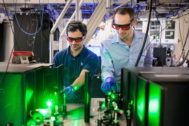
“Even if we have good control over where we put nitrogen, we always end up with this background noise,” Marcks said. “Because we want to grow highly coherent nitrogen vacancy centers, we wanted to better understand how these surrounding defects behave and couple with each other.” To better understand these single nitrogen electronic defects, the team used a laser and a home-built microscope system to measure the NV center. The number of photons that the NV center emits depends on the NV center’s spin state. Because these centers interact with other spins, the team realized they could use the NV center as a nanoscale sensor of the nearby nitrogen electron charge, which is otherwise invisible.
The process gave them the first-ever observation of coupled spin and charge dynamics within this material – right down to single defects. “We expected the nitrogen defects would all just have a single charge state, but they actually flip back and forth, and they are not always in the same charge state,” Marcks said. “That’s different from what we assumed from solid-state physics.” The team joined forces with Aashish Clerk and Giulia Galli, whose teams provided the theoretical and computational tools that allowed the researchers to better understand their observations.
Ultimately, the team will use this knowledge to not only better understand how these material systems behave but to also build better quantum sensors. “By combining experiment, theory, and computation, we have ideas on how to create extremely clean materials for emerging quantum technologies and control some of these internal noise sources,” Galli said. (Source: U. Chicago)
Link: Awschalom Group, Pritzker School of Molecular Engineering, University of Chicago, Chicago, USA


