Free-space optical light for high-speed wifi
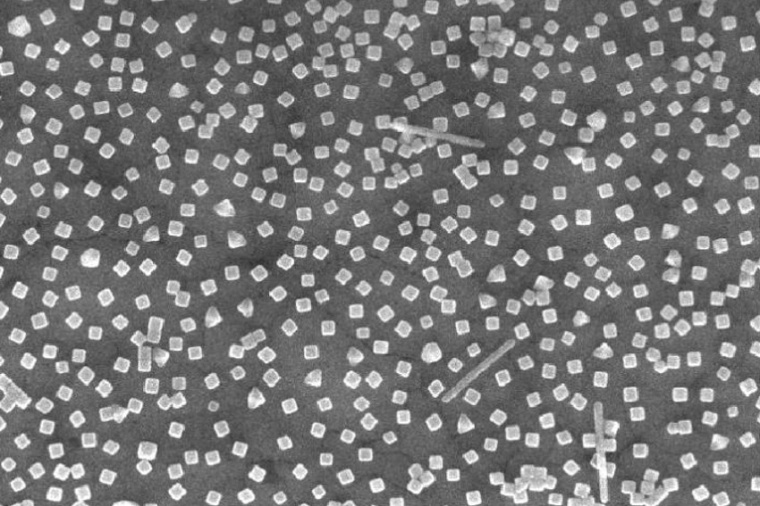
Nanocubes interact with the silver base in a way that enhances the photonic capabilities of the fluorescent dye.
Visible and infrared light can carry more data than radio waves, but has always been confined to a hard-wired, fiber-optic cable. Working with Facebook's Connectivity Lab, a Duke research team has now made a major advance toward the dream of ditching the fiber in fiber optics. While working to create a free-space optical communication system for high-speed wireless internet, the researchers also show that speed and efficiency properties previously demonstrated on tiny, single-unit plasmonic antennas can also be achieved on larger, centimeter-scale devices.
In 2016, researchers from Internet.org's Connectivity Lab outlined a new type of light detector that could potentially be used for free-space optical communication. Traditionally, hard-wired optical fiber connections can be much faster than radio wave wireless connections. This is because visible and near-infrared light frequencies can carry much more information than radio waves (WiFi, Bluetooth, etc). But using these higher frequencies in wireless devices is difficult. Current setups use either LEDs or lasers aimed at detectors that can reorient themselves to optimize the connection. It would be much more efficient, however, if a detector could capture light from different directions all at once. The catch is that increasing the size of an optical receiver also makes it slower.
This was also the case for the Connectivity Lab's design. A spherical bundle of fluorescent fibers captured blue laser light from any direction and re-emitted green light that could be funneled onto a small receiver. While the prototype was able to achieve rates of two gigabits per second, most fiber optic internet providers offer up to 10 Gb, and higher-end systems can push into the thousands. Looking for a way to speed up their free-space optical communication designs, the Connectivity Lab turned to Maiken Mikkelsen, the James N. and Elizabeth H. Barton Associate Professor of Electrical and Computer Engineering and Physics at Duke. Over the past decade, Mikkelsen has been a leading researcher in the field of plasmonics, which traps light on the surface of tiny nanocubes to increase a device's speed and efficiency at transmitting and absorbing light by more than a thousand times.
“The Connectivity Lab's prototype was constrained by the emissions lifetime of the fluorescent dye they were using, causing it to be inefficient and slow,” said Mikkelsen. “They wanted to increase the efficiency and came across my work showing ultrafast response times in fluorescent systems. My research had only proven that these efficiency rates were possible on single, nanoscale systems, so we didn't know if it could scale up to a centimeter-scale detector.” All previous work, Mikkelsen explains, has been proof-of-principle demonstrations with a single antenna. These systems typically involve metal nanocubes spaced tens to hundreds of nanometers apart and placed just a handful of nanometers above a metal film. While an experiment might use tens of thousands of nanocubes over a large area, research showing its potential for superfast properties has historically cherrypicked just one cube for measurement.
Now, Mikkelsen and Andrew Traverso, a postdoctoral researcher working in her laboratory, brought a more purposeful and optimized design to a large-area plasmonic device. Silver nanocubes just 60 nanometers wide are spaced about 200 nanometers apart, covering 17 % of the device's surface. These nanocubes sit just seven nanometers above a thin layer of silver, spaced by a coating of polymer that is jam-packed with four layers of fluorescent dye. The nanocubes interact with the silver base in a way that enhances the photonic capabilities of the fluorescent dye, causing a 910-fold increase in the overall fluorescence and a 133-fold emission rate enhancement. The superfast antenna also can capture light from a 120-degree field of view and convert it to a directional source with a record-high overall efficiency of 30 %.
“Plasmonic effects have always been known to lose a lot of efficiency over a large area,” said Traverso. “But we've shown that you can take attractive ultrafast emission features of a nanoscale device and recreate it on a macroscopic scale. And our method is very easily transferrable to fabrication facilities. We can create these largescale plasmonic metasurfaces in under an hour with pipettes and Petri dishes, just simple liquid depositions on metal films.”
The overall effect of the demonstration is the ability to capture light from a large field of view and funnel it into a narrow cone without losing any speed. To move forward with this technology, researchers would need to piece several plasmonic devices together to cover a 360-degree field of view and once again include a separate interior detector. While there is work to be done, the researchers see a viable path forward. “In this demonstration, our structure acts to efficiently relay the photons from a wide angle into a narrow angle without losing speed,” said Mikkelsen. (Source: Duke U.)
Link: Mikkelsen Lab, Dept. of Physics, Duke University, Durham, USA