Controlled laser drilling of microvias
25.06.2024 - HILaM research project develops process control of laser parameters for wider use of ultrashort pulse lasers
In the production of printed circuit boards (PCBs), micrometer-diameter vias – known as microvias – are drilled through multilayer PCBs. Lasers can drill through these structures with high throughput and micrometer precision. A measurement technique based on laser-induced breakdown spectroscopy (LIBS) is set to check the quality of the holes inline and control the process.
-
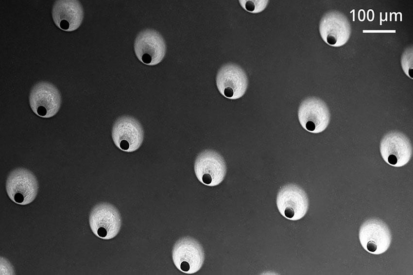 Vias in printed circuit boards have to be drilled with micrometer precision. A new measuring method is set to make it possible to control the microvias laser drilling process. (Source: 3D-Micromac)
Because of the high density of circuits and components, modern printed circuit boards are extremely challenging to manufacture. Lasers are used to drill the interconnects between the layers, or microvias, that are less than 200 µm in diameter. The drilling process must be fast, cost-effective, flexible and – most importantly – precise, because once the holes have been metalized, they form the electrical contact between the metal layers of the PCB. To ensure good contacting, the insulation material must be completely removed during the drilling process; this will determine the functionality and longevity of the electronic component. Currently, microvias quality control is usually a downstream step, which sometimes uses destructive methods such as cross-sectioning or electrical functional tests. What’s more, they are often just spot checks, which is not enough for safety-critical applications.
In the HILaM research project, Fraunhofer IPM, Chemnitz-based laser micromachining specialist 3D-Micromac, and Andus Elektronik from Berlin are developing an optical method for the inline quality control of microvias using ultrashort pulse (USP) lasers and the automatic control of the drilling process. The use of USP lasers to structure printed circuit boards has been on the rise because of their ability to produce holes with very small diameters in demanding materials and little space between the vias. USP lasers, however, are not selective in terms of material. This means that, with varying thickness and homogeneity of insulation layers, the drilling process requires precise control.
The researchers employ laser-induced breakdown spectroscopy (LIBS) to analyze and control the ablation process – pulse-resolved, selectively and spatially resolved within each hole. The LIBS sensor is integrated into the system coaxially to the laser and absorbs the plasma emissions of each material that are generated during ablation. The spectrum can be used to determine which material has been removed. If copper is present in the plasma spectrum, this means that the insulation layer has been sufficiently removed from the spot in question. The control algorithm then decides to move the laser to the next position within the hole. This ensures one hundred percent inline quality control.
Contact
*Fraunhofer-Institut für Physikalische Messtechnik IPM
Georges-Köhler-Allee 301
79110 Freiburg
Germany