Metalenses focus light with ultra-deep holes
New approach improves the impedance match between the incident and transmitted waves
Metasurfaces are nanoscale structures that interact with light. Today, most metasurfaces use monolith-like nanopillars to focus, shape and control light. The taller the nanopillar, the more time it takes for light to pass through the nanostructure, giving the metasurface more versatile control of each color of light. But very tall pillars tend to fall or cling together. What if, instead of building tall structures, you went the other way? Now, researchers at the Harvard John A. Paulson School of Engineering and Applied Sciences (SEAS) developed a metasurface that uses very deep, very narrow holes, rather than very tall pillars, to focus light to a single spot.
-
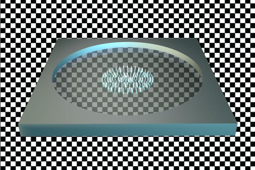 Illustration of a holey metalens. (Source: Capasso Lab, Harvard SEAS)
The new metasurface uses more than 12 million needle-like holes drilled into a 5-micrometer silicon membrane. The diameter of these long, thin holes is only a few hundred nanometers, making the aspect ratio nearly 30:1. It is the first time that holes with such a high aspect ratio have been used in meta-optics. “This approach may be used to create large achromatic metalenses that focus various colors of light to the same focal spot, paving the way for a generation of high-aspect ratio flat optics, including large-area broadband achromatic metalenses,” said Federico Capasso, the Robert L. Wallace Professor of Applied Physics and Vinton Hayes Senior Research Fellow in Electrical Engineering at SEAS.
“If you tried to make pillars with this aspect ratio, they would fall over,” said Daniel Lim, a graduate student at SEAS. “The holey platform increases the accessible aspect ratio of optical nanostructures without sacrificing mechanical robustness.” Just like with nanopillars, which vary in size to focus light, the holey metalens has holes of varying size precisely positioned over the 2 millimeters lens diameter. The hole size variation bends the light towards the lens focus.
“Holey metasurfaces add a new dimension to lens design by controlling the confinement and propagation of light over a wide parameter space and make new functionalities possible,” said Maryna Meretska, a postdoctoral fellow at SEAS. “Holes can be filled in with nonlinear optical materials, which will lead to multi-wavelength generation and manipulation of light, or with liquid crystals to actively modulate the properties of light.”
The metalenses were fabricated using conventional semiconductor industry processes and standard materials, allowing it to be manufactured at scale in the future. The Harvard Office of Technology Development has protected the intellectual property relating to this project and is exploring commercialization opportunities. (Source: Harvard SEAS)
Link: Capasso Group, Harvard John A. Paulson School of Engineering and Applied Sciences, Cambridge, USA